


Introduction
Every company here meets three editorial filters: a genuine UK presence or substantial UK-based manufacturing and R&D; a real photonics specialism rather than general electronics distribution; and a verifiable commercial track record.
Each entry is assessed across four consistent axes: core technology specialism, application verticals served, supply-chain position (component maker, system integrator, OEM supplier, or research-commercialisation spinout), and the depth of UK presence and manufacturing.
One distinction worth keeping in mind: a company that designs, builds, and supports its own technology in-house tells a different story about engineering depth than one that resells or imports.
The entries follow a consistent structure throughout, making it straightforward to scan and compare — starting with a UK photonics manufacturer anchoring the list at position one.
TL;DR
The UK photonics sector is far more varied than a simple technology list suggests — it spans in-house manufacturers with deep research heritage, upstream foundries, specialist spinouts, and imaging pioneers, each occupying a distinct position in the supply chain.
Knowing where a company sits matters as much as knowing what it makes.
This article covers:

Notable UK photonics companies across key sub-sectors
Inclusion criteria and evaluation axes used
Supply-chain positions: manufacturer, integrator, foundry, spinout
Application verticals each company serves
UK sector scale, clusters, and growth context
Matching company type to your specific need
Photonics companies UK: understanding the sector landscape
UK photonics is not a niche academic pursuit — it is a £18.5 billion industry that grew 20% in just two years and contributes £8.6 billion in GVA to the broader economy, according to the Photonics Leadership Group's evidence pack and the Council for Science and Technology's 2026 advice to the Prime Minister.
Globally, the UK ranks ninth largest photonics market and second in Europe, behind only Germany — a position that reflects genuine industrial depth rather than research reputation alone.
That depth is reinforced by the sector's export intensity: over half of UK photonics firms export more than 75% of their output, making UK-based companies natural candidates for international supply-chain partnerships.
Much of this activity is organised around distinct regional clusters, each shaped by a combination of university research heritage, infrastructure investment, and accumulated industrial expertise.
- Southampton: Home to internationally leading silicon photonics capability, with deep optical fibre heritage rooted in the Optoelectronics Research Centre (ORC).
- Glasgow and Scotland: A long-established photonics cluster generating over £1.2 billion annual turnover, with GaN micro-LED leadership at Strathclyde's Institute of Photonics.
- Bristol and South Wales: A compound semiconductor hub anchored by the REWIRE IKC at Bristol and the world's first dedicated compound semiconductor cluster in South Wales.
- Northern Ireland: Home to Queen's University Belfast, listed among the UK's recognised university clusters for photonics research activity.
Government investment has reinforced these clusters deliberately: the National Semiconductor Strategy directed £11 million each to the Cornerstone IKC in Southampton (silicon photonics) and the REWIRE facility at Bristol (compound semiconductors), while the National Quantum Strategy commits £2.5 billion over ten years from 2024 to quantum technologies — a programme in which photonics plays a central enabling role.
The Photonics Leadership Group coordinates sector representation, and over 1,650 company operating sites are active across the UK alongside more than 40 universities and 18 research and training organisations.
Where UK firms are most active tells its own story: industrial laser materials processing, high-value supply chain components such as optical fibre, and medical and life sciences — technology applied across drug discovery, diagnostics, and treatment.
The UK's strongest photonics companies frequently trace their engineering directly to pioneering university labs — Southampton's ORC, Heriot-Watt, the Strathclyde Institute of Photonics, and Queen's University Belfast among them. That institutional lineage is a reliable indicator of technical depth that catalogue suppliers cannot replicate.
The sector's trajectory reinforces the case for paying attention to it: growing at 4.4% per year, with a projected value of £50 billion by 2035 and the potential to support up to 150,000 additional jobs, according to the Council for Science and Technology.
The five companies profiled below represent the breadth of that ecosystem — spanning different clusters, technology sub-sectors, and positions in the photonics supply chain.
Company 1
Woodrow Scientific Limited — custom EDFA manufacturer, Southampton

Southampton-based Woodrow Scientific Limited designs and manufactures custom erbium-doped fibre amplifiers (EDFAs) built end-to-end to the customer's application, with power scalability reaching the highest commercially available levels.
Pros:

Fully engineered to the application, not off-the-shelf
Scales to 200 W+ average, 100 kW+ peak
In-house design, build, and support on patented technology
Air-cooled as standard; no chiller required
Cons:

Each unit is quoted per project, not catalogue-priced
Woodrow Scientific Limited (WSL) was founded in 2012 by a fibre-laser specialist holding a PhD from Southampton's Optoelectronics Research Centre — the institution where the erbium-doped fibre amplifier was first demonstrated.
That lineage is not incidental: WSL's team and network work closely with the people who pioneered EDFA technology, and the company has grown to more than 20 laser specialists, with the headcount continuing to rise.
Custom EDFA: engineered to the application
WSL's primary photonics credential is its Custom EDFA platform — erbium-doped fibre amplifiers built to a MOPA architecture across the full 1530–1625 nm window, covering C-band (1530–1565 nm), L-band (1565–1625 nm), or dual C+L.
What distinguishes WSL's approach is the depth of tailoring applied to every unit: operating band, output power, pulse regime, pulse energy and peak power, cooling configuration, delivery cable length and termination, form factor, and control firmware are all configured per project, not selected from a fixed catalogue.
On power, WSL builds to the leading commercially available levels — average powers reaching 200 W or more, pulse energies above 10 mJ, and peak powers above 100 kW, with output fully tunable from 0 to 100% of rated power.
WSL's EDFA platform reaches average powers of 200 W or more, pulse energies above 10 mJ, and peak powers above 100 kW — with output controllable across the full 0–100% range. These are the highest average power levels commercially available in this class.
The platform operates at 1550 nm, an eye-safer wavelength than legacy 1064 nm sources, and reduced-hazard-zone builds are available for deployments where the operational safety envelope is a design constraint.
Air-cooled operation is standard across the range, which removes the need for a chiller or coolant loop and simplifies integration into customer systems; water cooling is available for those whose thermal management architecture calls for it.
- Operating band: C-band, L-band, or dual C+L — both delivered through a single cable from one source.
- Pulse regime: CW, short-pulse (e.g. 100–500 ns), or custom — specified per project.
- Cooling: Air-cooled as standard; water cooling available as an option.
- Form factor: Custom integration envelope, delivery cable length and termination configured to the application.
- Control firmware: Custom firmware and communication standards specified per project.
- Certifications: CE and UKCA certified.
WSL's engineers provide direct support throughout the integration process — a meaningful practical benefit given the complexity of embedding a high-power fibre amplifier into a demanding system.
Application verticals
The EDFA platform serves a broad range of technically demanding verticals, including free-space optical communications (FSOC) and ground-station uplink, LiDAR, quantum sensing and communications, defence and directed-energy, remote sensing, distributed acoustic sensing, scientific instrumentation, and medical applications.
WSL technology is part of global space programmes today; programme and customer names are confidential.
Supply-chain position: in-house manufacturer
A meaningful distinction when mapping the UK photonics supply chain is whether a supplier designs and builds its own products or sources and resells them — the two models carry very different implications for engineering support, customisation depth, and long-term product ownership.
WSL designs, manufactures, qualifies, and supports its amplifiers entirely in-house, on patented technology: 10 patents and counting, backed by more than 200 years of combined engineering experience across the team.
Products ship worldwide direct from Southampton, with no intermediary in the supply chain between WSL's engineers and the end customer.
Laser cleaning: WSL's second field
Alongside its EDFA work, WSL operates in laser cleaning, producing the portable ELASER and the automated AutoLASE — both incorporating what WSL describes as world-first eye-safe laser cleaning technology.
The cleaning systems are designed for industrial use across all sectors, and WSL also supplies amplifiers on an OEM basis to customers building their own laser cleaning systems, using the EDFA as the engine.
Specifications and pricing for the Custom EDFA are quoted per project: prospective customers submit their requirements for a specialist evaluation by WSL's engineering team.
Custom EDFAs built to your application
Woodrow Scientific designs and manufactures tailored erbium-doped fibre amplifiers for laser communications, free-space optical links, and beyond. Explore the full range of custom EDFA solutions.

Company 2
M Squared Lasers
Glasgow-based M Squared designs and manufactures advanced laser platforms and integrated quantum systems, serving scientific research institutions and quantum technology programmes across the UK and internationally.
Pros:
SolsTiS platform holds IoP and Queen's Award
Spans CW, ultrafast, mid-IR and THz platforms
UK's first commercial quantum gravimeter and accelerometer
Verticals span quantum, biophotonics, defence, space
M Squared was founded in 2006 by Dr Graeme Malcolm OBE and Dr Gareth Maker at the West of Scotland Science Park in Glasgow, drawing on a lineage that traces back to Microlase Optical Systems, a Strathclyde University spinout the pair co-founded in 1992.
Glasgow's photonics cluster provided the environment for M Squared to develop what became its flagship platform: the SolsTiS, a continuous-wave Ti:Sapphire laser that the company describes as a step-change in CW Ti:Sapphire laser technology.
The SolsTiS Platform
Ti:Sapphire lasers are valued in quantum research for two properties that are difficult to achieve simultaneously: extremely narrow linewidth and broad wavelength tunability. The SolsTiS delivers both in a sealed, alignment-free cavity small enough to sit on a laboratory bench.
M Squared's own published datasheets specify a tuning range of 670–1050 nm with more than 300 nm of continuous tuning from a single optics set and a passive linewidth below 50 kHz; with active feedback, linewidths below 10 Hz have been achieved.
The platform can be extended via frequency conversion modules to cover 210 nm to 4 µm, giving researchers access to deep UV through mid-IR wavelengths from a single coherent source. SolsTiS received a 2015 Business Innovation Award from the Institute of Physics and the Queen's Award for Enterprise in Innovation in 2016.
Laser Platform Portfolio
Beyond SolsTiS, M Squared offers a portfolio covering ultrafast and infrared regimes.
- Sprite XT: A tunable femtosecond Ti:Sapphire laser covering 720–980 nm, delivering more than 1.5 W at peak with pulse durations below 150 fs. Suited to multiphoton excitation, time-resolved spectroscopy, and quantum optics experiments.
- Firefly IR: A pulsed, tunable mid-infrared source spanning 1.4–8.5 µm across the model family, designed for molecular spectroscopy, remote sensing of hydrocarbons, and standoff gas detection.
- Firefly THz: A compact terahertz laser source with widely tunable, narrow-linewidth output, intended for remote sensing and spectroscopy applications where post-detection Fourier processing is impractical.
- SolsTiS Titan: A fully automated, high-power single-frequency variant of the SolsTiS platform operating in the UV and visible, qualified for 24/7 industrial use in semiconductor writing, inspection, and quantum applications.
Taken together, the portfolio spans CW to femtosecond pulse regimes and deep UV to terahertz wavelengths — a breadth that M Squared describes as covering expertise from CW to fs and DUV to THz.
Quantum Systems Integrator
M Squared explicitly positions itself as a quantum technology systems integrator, not merely a laser supplier. Its quantum brochure states that the company sits at the heart of the international quantum supply chain, developing components, sub-systems, and sensors for commercial quantum applications.
Three complete quantum instruments have been developed, each built on the SolsTiS laser platform as its optical foundation.
- Quantum Gravimeter: Described by M Squared as the first commercial quantum gravimeter built by a UK company, it uses atom interferometry to measure local gravitational acceleration with high precision. Applications include mineral prospecting, underground infrastructure assessment, archaeology, and geodesy.
- Quantum Accelerometer: The UK's first commercial quantum accelerometer for navigation, it measures horizontal accelerations using atom interferometry without reliance on satellite signals. Target applications include navigation for ships, submarines, and autonomous underwater vehicles.
- Optical Lattice Clock: A compact, transportable strontium lattice clock for precision timekeeping. M Squared describes the project as aiming to create the world's first commercially available fully integrated optical frequency atomic clock.
This systems-layer role distinguishes M Squared from companies that supply laser components into others' quantum instruments: M Squared designs, builds, and delivers the complete quantum instrument.
Application Verticals
M Squared's platforms serve a wide range of application areas, as documented across its own published pages: quantum computing and sensing, biophotonics and biomedical research, chemical sensing, defence and security, space technology, oil and gas, advanced manufacturing, and semiconductor metrology.
The biophotonics vertical is handled through a dedicated division, M Squared Life, established in 2015 at the Surrey Research Park in Guildford. Its primary product is the Aurora, an Airy Beam light sheet fluorescence microscope designed for 3D volumetric imaging in neuroscience, developmental biology, cancer biology, and regenerative medicine research.
In the defence and chemical sensing vertical, the Firefly IR platform is deployed for standoff detection of threat agents and fugitive gas emissions, as well as remote sensing of hydrocarbons in oil and gas environments.
UK Presence
M Squared's headquarters remain at 1 Kelvin Campus, West of Scotland Science Park, Glasgow, where the company was founded. A dedicated UK Quantum Centre operates from Inovo, 121 George Street, Glasgow, focused on quantum product development and commercialisation.
A London office at Here East, Queen Elizabeth Olympic Park, Stratford, extends the company's footprint into the capital's technology corridor. M Squared's awards page records that SolsTiS is used by over 200 organisations in 30 countries, reflecting the international reach of its laser platforms.
M Squared holds over 230 patents, according to its published quantum brochure, with the SolsTiS platform recognised by the Royal Academy of Engineering as a MacRobert Award finalist in 2019.
The company's awards record is extensive: alongside the IoP Business Innovation Award and the Queen's Award for Enterprise in Innovation (2016) and International Trade (2017), M Squared has topped the Metis IP100 intellectual property league table for three consecutive years.
Company 3
Photon Force — SPAD array cameras and sensing, Edinburgh
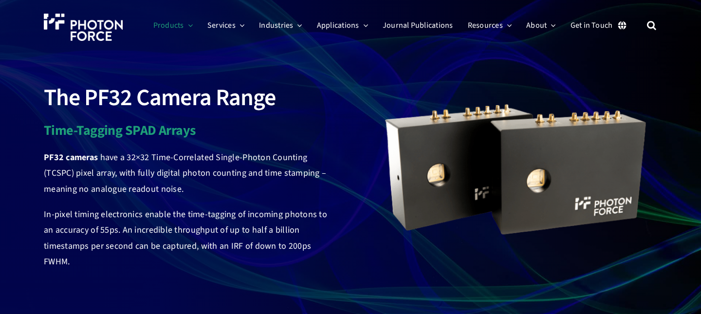
Edinburgh-based designer and manufacturer of SPAD array cameras and sensors, timestamping up to 500 million photons per second at 55 ps resolution, serving photonics R&D, LiDAR, quantum optics, biomedical research, and defence applications.
Pros:
500M photon timestamps per second throughput
55 ps timing resolution across 1,024 pixels
Spans R&D, quantum, biomedical and defence verticals
Custom OEM sensor and ROIC design service available
Cons:
Highly specialist technology; not a general-purpose camera
Targets research and specialist industrial markets
Photon Force was founded in 2015 by Dr Richard Walker, drawing on seven years in the renowned CMOS Sensors and Systems Group at the University of Edinburgh, and it remains headquartered at Murchison House on Edinburgh's scientific campus — adding a second Scottish address to this list, distinct in character from the Glasgow laser platforms covered in the preceding entry.
The company's focus is singular: designing and manufacturing Single-Photon Avalanche Diode (SPAD) array cameras and sensors that can detect, count, and time the arrival of individual photons at speeds no conventional imaging sensor can approach.
The PF32 Platform: Technology and Performance
A SPAD works by triggering an avalanche of current the instant a single photon strikes the detector — an event the surrounding electronics register and timestamp in picoseconds. In a SPAD array, hundreds of these detectors operate simultaneously and independently, turning what was once a single-channel measurement into a full imaging capability.
Photon Force's flagship product line, the PF32, places a 32×32 array of these pixels into a compact camera body, with each pixel capable of timestamping incoming photons to an accuracy of 55 picoseconds. Combined with high-speed readout, the platform delivers up to 500 million photon timestamps per second — a throughput figure the company describes as unparalleled in the marketplace.
The technique underpinning this is Time-Correlated Single Photon Counting (TCSPC): each detected photon is timestamped relative to a synchronisation reference, typically a pulsed laser, producing time-of-flight or fluorescence decay data with exceptional precision. Photon Force's FAQ notes that while other TCSPC systems may offer finer temporal resolution, none deliver it simultaneously across 1,024 independent channels.
The PF32 range currently spans multiple models — including Lite, Core, and Ultra variants — each available with or without a microlens option that raises the effective fill factor and increases photon collection efficiency.
Application Verticals: One Platform, Many Fields
The underlying reason a single sensor platform can serve such a wide range of disciplines is that the ability to timestamp individual photons at high speed is a fundamental requirement across many fields — wherever light levels are too low for conventional detectors, or where the precise timing of photon arrivals carries the information of interest.
- Photonics R&D: Fluorescence spectroscopy, Raman spectroscopy, ultrafast laser fabrication research, and the development of LiDAR systems and optical waveguide components.
- Biomedical research: Fluorescence Lifetime Imaging Microscopy (FLIM), Diffuse Correlation Spectroscopy (DCS), brain-computer interfaces, and functional near-infrared spectroscopy — applications where capturing photon decay times at video rate was previously impractical.
- Quantum optics: Multi-channel Quantum Key Distribution (QKD), entangled photon correlation measurements, and quantum-enhanced imaging.
- LiDAR and 3D imaging: High-resolution time-of-flight ranging, non-line-of-sight imaging (tracking hidden objects around corners), and imaging through scattering media.
- Defence and security: Long-range drone and UAS detection using the high-frequency rotor-blade signature captured by the PF32's fast frame rate.
The drone detection application illustrates the technology's reach in concrete terms. Rather than trying to resolve a distant object spatially, the PF32 uses its inherent high frame rate to extract the characteristic flicker frequency of a drone's rotating blades from photon arrival data — identifying the target by how its light behaves over fractions of a nanosecond, rather than by what it looks like.
Photon Force's technology positions the PF32 as a platform where the timing of individual photon arrivals is itself the measurement — enabling applications from imaging around corners to detecting drones at long range that single-channel detectors cannot address.
Photon Force describes the combination of 55 ps timing resolution and 500 million timestamps per second as unparalleled in the marketplace, attributing this to an architecture in which timing electronics are embedded within each pixel, delivering unparalleled throughput across all 1,024 channels simultaneously.
Supply-Chain Position: Manufacturer and OEM Partner
Photon Force is a designer and manufacturer of its cameras and sensors. Its 2024 brochure confirms that alongside the finished PF32 camera range, the company offers a design and manufacturing service for custom sensors and readout integrated circuits (ROICs), spanning resolution, size, and architecture options.
This means the company serves two distinct customer types: research institutions and laboratories purchasing finished instruments from the PF32 range, and commercial product developers who need a custom single-photon sensor built into their own system. The OEM module version of the PF32 — a compact, low Size, Weight and Power format — was developed specifically to support volume production of embedded products.
The company operates worldwide and has been accelerating customer research internationally since 2015, with its technology used across fields spanning neuroscience, communications, energy, and automotive, in addition to its core scientific research base.
Company 4
IQE plc — compound semiconductor wafer manufacturer, Cardiff

Cardiff-headquartered IQE plc is the world's leading pure-play epitaxial wafer manufacturer, supplying compound semiconductor epiwafers that underpin photonics devices across AI data centres, consumer 3D sensing, defence infrared, and space.
Pros:
World's only scaled pure-play epitaxy provider
Broad material platforms: InP, GaAs, GaSb, GaN
Long-term strategic agreements with tier-1 customers
Over 35 years of compound semiconductor pedigree
Cons:
Upstream foundry; supplies wafers, not finished devices
B2B only; no direct route for most buyers
Capital-intensive model with high barriers to entry
IQE plc sits at the base of the photonics supply chain: it manufactures the compound semiconductor epitaxial wafers (epiwafers) from which device makers build lasers, detectors, VCSELs, and other photonic components.
Founded in Cardiff in 1988 as Epitaxial Products International, the company describes itself as the leading global supplier of compound semiconductor wafer products — a position it attributes to being the world's only pure-play epitaxy provider with a scaled global manufacturing footprint.
IQE's role in the supply chain is distinct from every other company in this guide: it supplies epiwafers to device manufacturers, fabless designers, and OEMs, who then build the photonic components and systems that reach end markets.
Technology and Material Platforms
IQE grows epiwafers using Metal Organic Chemical Vapour Deposition (MOCVD), Molecular Beam Epitaxy (MBE), and Chemical Vapour Deposition (CVD), and describes itself as the only company with mass production capability across both MOCVD and MBE for III-V compound semiconductors.
- Indium Phosphide (InP): The platform underpinning fibre-optic transceivers and next-generation optical interconnects for AI and hyperscale data centres. IQE has produced InP epiwafers since its inception and has expanded its portfolio to 6-inch wafers to support scaling in datacom.
- Gallium Arsenide (GaAs): The material platform behind VCSELs for 3D facial recognition and consumer sensing in smartphones and tablets, as well as optical communication lasers and photodetectors. IQE also supplies GaAs epiwafers for quantum dot laser foundry services targeting AI data centre interconnects.
- Gallium Antimonide (GaSb): The specialist platform for mid-wave and long-wave infrared detection. IQE describes itself as the world leader in antimonide materials, supplying GaSb epiwafers for military surveillance, border security, and space imaging applications.
- Gallium Nitride (GaN): A wide-bandgap platform used in radar, electronic warfare, and 5G base station power amplifiers. IQE supplied the first commercial GaN HEMT epiwafer more than 20 years ago and continues to scale GaN across multiple substrate platforms.
IQE also provides quantum dot laser (QDL) foundry services through its partnership with Quintessent Inc., supplying 6-inch GaAs epiwafers for a laser technology designed to address power and latency demands in AI data centre optical interconnects.
Application Verticals
The breadth of IQE's material platforms translates into downstream reach across a wide range of end markets.
In AI and hyperscale data centres, InP epiwafers enable the optical transceivers and photonic interconnects that carry data at high speeds; IQE has described accelerating InP demand as a material growth driver for the business.
GaAs VCSELs produced from IQE wafers power the 3D sensing systems in smartphones and tablets — including facial recognition and gesture detection — and the automotive LiDAR and in-cabin sensing platforms that are expanding the application beyond consumer mobile.
In aerospace and defence, GaSb and InP wafers enable the long-wavelength infrared detectors, quantum cascade lasers, and radar systems used in surveillance, threat detection, and secure satellite communications.
Automotive sensing and industrial automation draw on GaAs VCSEL and GaN platforms for LiDAR, radar, and power electronics, while wireless infrastructure — from 5G base stations to satellite internet constellations — relies on GaN RF epiwafers.
In December 2025, IQE extended a multi-year strategic supply agreement with Lumentum Holdings Inc., a global photonics technology company. The agreement covers VCSEL epiwafers supporting 3D sensing, consumer, and automotive LiDAR applications, building on a longstanding relationship between the two companies.
The Lumentum agreement is one example of the long-term, high-volume supply arrangements that characterise IQE's customer relationships — a structural feature of the epiwafer business that reflects both the technical complexity of qualifying a new wafer supplier and the capital commitment required on both sides.
UK Presence and Scale
IQE's registered office and Innovation Centre are located at Pascal Close, St Mellons, Cardiff — the same city where its first MOCVD manufacturing operation was established in 1988.
Its Newport facility, on Celtic Way in Marshfield, is a large-scale compound semiconductor foundry developed as part of the South Wales compound semiconductor cluster — a regional ecosystem anchored by IQE and supported by Cardiff University, the Compound Semiconductor Applications Catapult, and UK and Welsh Government investment.
A third UK site in Milton Keynes (IQE Wafer Technology) handles substrate manufacturing, complementing the epitaxial operations in Cardiff and Newport.
IQE is listed on the AIM Stock Exchange in London and has additional manufacturing in the US and Taiwan, giving it the global supply security and scalability that underpins its position as a foundry partner for major chip and OEM customers.
IQE's photonics business has grown year-on-year, with the company reporting increased photonics revenue in its FY2025 full-year results, driven by demand across its InP, GaAs, and GaSb platforms.
With over 35 years of compound semiconductor expertise and a market position defined by high barriers to entry — the capital intensity, process complexity, and customer qualification cycles of epitaxial wafer manufacturing are substantial — IQE represents a foundational tier of the UK photonics industrial base that has few direct comparators anywhere in the world.
Company 5
Andor Technology (Oxford Instruments Andor), Belfast
Oxford Instruments Andor is a Belfast-based manufacturer of scientific imaging cameras, spectroscopy solutions, and microscopy systems, spun out from Queen's University Belfast in 1989 and acquired by Oxford Instruments in 2014.
Pros:
Four camera platforms: EMCCD, sCMOS, CCD, intensified
Cameras used in SOFIA, RAVEN, SuperWASP programmes
10,000+ customers across 55 countries worldwide
Strong OEM partner capability for instrument manufacturers
Cons:
Products positioned as high-performance research instrumentation
2024 rebrand creates a brand-recognition transition
Oxford Instruments Andor designs and manufactures scientific imaging cameras, spectroscopy platforms, and microscopy systems from its purpose-built facility in Belfast, serving research institutions and instrument manufacturers across the physical and life sciences.
From Queen's University Belfast to Global Scale
Andor was born out of Queen's University Belfast in 1989 — a textbook example of the UK's university spinout model maturing into a globally significant company.
From its origins in a university laboratory, Andor has grown to over 10,000 customers in 55 countries, with more than 70 unique product solutions, 400 staff, and 16 offices worldwide. Oxford Instruments acquired the company in 2014, and in 2024 it rebranded as Oxford Instruments Andor to align with the wider group identity.
The rebrand, announced in 2024, does not affect the product range or level of support — its purpose is to leverage the combined global footprint of the Oxford Instruments group across key markets.
Core Technology: Cameras, Detectors, and Spectroscopy
Andor's camera portfolio spans four principal sensor technologies, each targeting distinct performance requirements across light levels, speed, and spectral range.
| Platform | Key Characteristic | Typical Applications |
|---|---|---|
| EMCCD | Single photon sensitivity, back-illuminated QE >95%, TE cooling to -100°C | Single molecule detection, low-light astronomy, quantum optics |
| sCMOS | Multi-megapixel, low noise, high frame rates, large field of view | Fast time-resolution astronomy, adaptive optics, live cell imaging |
| CCD (slow-scan) | TE cooling to -100°C, industry-leading low noise, large area sensors | Long-exposure spectroscopy, photometric surveys, deep-field imaging |
| Intensified / Gated (ICCD) | Optical gating to <2 ns, UV to SWIR response, fibre-coupled intensifiers | Plasma diagnostics, LIBS, transient spectroscopy, quantum entanglement studies |
Andor's four main camera platforms compared across their defining performance characteristics and primary application areas, as described on Andor's own product pages.
On the spectroscopy side, Andor's spectrograph family is based on Czerny-Turner and Echelle optical designs, covering UV to SWIR wavelengths with configurations suited to everything from Raman and photoluminescence to LIBS and plasma emission spectroscopy.
The Kymera and Shamrock Czerny-Turner platforms offer high modularity and intelligent motorisation; the Mechelle Echelle platform provides simultaneous broadband coverage with high spectral resolution, particularly suited to LIBS and plasma science.
Application Verticals
Andor's product range addresses demanding research and industrial applications across two broad domains.
- Physical science: Quantum optics, plasma science, material science, chemistry, catalysis, fluid physics, and astronomy — from sub-atomic studies to imaging distant galaxies.
- Life science and biomedical: Single molecule detection, fluorescence microscopy, super-resolution imaging, drug discovery, drug safety and efficacy studies, and cancer research.
- Astronomy and space: The iXon EMCCD range has been used in the RAVEN multi-object adaptive optics system at the Subaru Telescope (Hawaii), CHIMERA (the Caltech high-speed multi-colour camera for Kuiper Belt object detection), and SOFIA, NASA's large-scale airborne observatory. The iKon-L 4-megapixel CCD has been the mainstay detector for the SuperWASP and Next-Generation Transit Survey exoplanet programmes.
- OEM industrial instrumentation: Cameras, spectrographs, and microscopy sub-systems integrated into third-party analytical, laboratory, and medical diagnostic instruments worldwide.
The breadth of that application footprint — from single-molecule biology to space observatory instrumentation — is one of the more striking features of Andor's portfolio relative to most specialist photonics instrument makers.
Supply-Chain Position and Belfast Facility
Andor is a designer and manufacturer, not a reseller: its cameras, detectors, spectrographs, and integrated microscopy systems are engineered and built in-house.
The company also operates as an OEM partner for instrument manufacturers integrating photon-detection capability into their own products — supplying standard, tailored, and fully custom camera and spectroscopy solutions, supported by dedicated OEM account management and engineering teams.
The principal manufacturing and R&D base is a purpose-built 50,000 sq ft facility in Belfast, which includes optical, electronic, and mechanical workshops alongside a 3,000 sq ft clean room and vacuum and electronic processing facilities.
Andor sits as one of seven businesses within the Oxford Instruments group, which is headquartered in the UK — placing Belfast-based manufacturing within a broader UK-anchored scientific instrumentation group with operations in 23 countries.
Conclusion
Mapping your path through the UK photonics sector
The sharpest navigational insight this list offers is not a name — it is a category: knowing whether you need an upstream foundry, a systems integrator, a research-grade sensing specialist, or a manufacturer who builds to your specification is the decision that shapes everything else.
For high-power fibre amplification or laser cleaning, Woodrow Scientific Limited is where this page points — an in-house UK manufacturer engineering every amplifier end-to-end to the application, not sourcing from a catalogue.
The sector itself is moving quickly, backed by sustained government investment, and the range of companies active within it will only grow.
Frequently asked questions about UK photonics companies
The questions below address common queries about the UK photonics sector — its scale, its leading companies, and how to navigate the landscape as a buyer or partner.
Component manufacturers supply precision parts — fibre amplifiers, compound semiconductor wafers, SPAD sensors, detectors — that are integrated into larger systems. System integrators deliver complete, ready-to-deploy solutions. The right choice depends on whether you need a building block or a finished capability. If you know your system architecture and need a specific component, look to a specialist manufacturer with deep in-house engineering: one that designs, builds, qualifies, and supports its own technology rather than repackaging catalogue parts. If you need a complete system and lack in-house integration resource, a system integrator is the more appropriate starting point. Some companies in the UK photonics sector occupy both positions to varying degrees, so it is worth clarifying exactly what a supplier delivers before engaging.
Notable UK photonics companies span a wide range of sub-sectors and supply-chain positions — there is no single definitive ranking, and the right answer depends on the application and what you need. This page applies three editorial criteria: UK presence or substantial UK operations, genuine photonics specialism, and verifiable commercial activity. The companies featured here — spanning fibre amplification, quantum laser platforms, single-photon sensing, compound semiconductor wafer manufacturing, and scientific imaging — represent the breadth of the sector rather than a size-ordered list. The UK photonics industry includes over 1,650 company operating sites, so any curated selection is necessarily a starting point for further research rather than an exhaustive directory.
The UK has particular depth in several photonics sub-sectors. Optical fibre and amplification is a historic strength, rooted in the University of Southampton's Optoelectronics Research Centre, where the erbium-doped fibre amplifier was first demonstrated. Industrial laser materials processing is another area of established commercial scale. Semiconductor photonics spans compound semiconductors — concentrated in South Wales and Bristol — and silicon photonics, where the Cornerstone IKC at Southampton provides national rapid-prototyping capability. Quantum photonics is a growth area backed by the National Quantum Strategy, with notable clusters in Glasgow and Edinburgh. The UK also has recognised strength in medical and life sciences photonics and in space and satellite applications. The sector is growing at 4.4% per year, with government-backed investment in quantum and semiconductor photonics accelerating activity across several of these areas.
In the UK, photonic chip development spans foundries, fabless designers, and research institutions. IQE plc, headquartered in Cardiff, is a foundational example at the supply-chain base: its compound semiconductor epiwafers underpin photonic devices including VCSELs and InP-based components used in optical interconnects and photonic chip architectures for AI data centres and optical communications. On the silicon photonics side, the Cornerstone IKC at the University of Southampton — a research facility rather than a commercial company — provides an open-access silicon photonics foundry serving collaborators in over 20 countries, with applications spanning telecoms, quantum technologies, AI hardware, and LiDAR. The broader photonic chip ecosystem extends well beyond any single organisation and includes fabless designers and OEM device manufacturers across the UK's established semiconductor clusters.
The UK has the second-largest photonics industry in Europe (after Germany) and the ninth-largest globally, according to the Photonics Leadership Group's evidence pack. The sector achieved £18.5 billion turnover in 2024, up 20% over two years, and contributes £8.6 billion in GVA to the economy. It employs 84,000 people — more than aerospace or motor manufacturing. The sector is growing at 4.4% per year, with the potential to reach £50 billion in value by 2035. Export intensity is high: over half of UK photonics firms export more than 75% of their output. Government investment reinforces this trajectory — the National Quantum Strategy commits £2.5 billion over ten years, and the National Semiconductor Strategy targets world-leading strength in compound semiconductors and silicon photonics, both of which are central to the photonics supply chain.