

Introduction
This guide is written for engineers, researchers, and technical evaluators who want a rigorous, working understanding of semiconductor optical amplifier technology — not a surface-level overview, and not an academic treatise.
It moves from the underlying physics and device structures through to performance parameters, design trade-offs, and real-world applications, building a picture that is useful whether you are specifying a component, evaluating a platform, or simply filling a gap in your knowledge.
The aim throughout is precision without unnecessary complexity — the kind of clarity that comes from knowing a subject well enough to explain it plainly.
TL;DR
Semiconductor optical amplifiers occupy a genuinely distinct position in the optical amplifier landscape: their chip-scale form factor makes them uniquely suited to photonic integration and signal processing, but they carry real trade-offs in noise and output power relative to fibre-based alternatives.
The right amplifier choice is always application-specific — and understanding why requires getting into the physics and engineering of how SOAs actually work.
This article covers:

Operating principles and carrier dynamics
SOA device types and structural taxonomy
Gain, noise figure, and saturation parameters
Polarisation sensitivity causes and mitigation
SOA vs. EDFA: honest engineering trade-offs
Applications, photonic integration, emerging uses
What is a Semiconductor Optical Amplifier?
At its core, a semiconductor optical amplifier does something deceptively straightforward: it takes an optical signal and makes it stronger, using a chip-scale semiconductor device rather than kilometres of specialised fibre or a separate high-power pump laser. That simplicity of premise, combined with a surprisingly broad reach across wavelength bands and application domains, is what makes the SOA one of the most versatile devices in modern photonics.
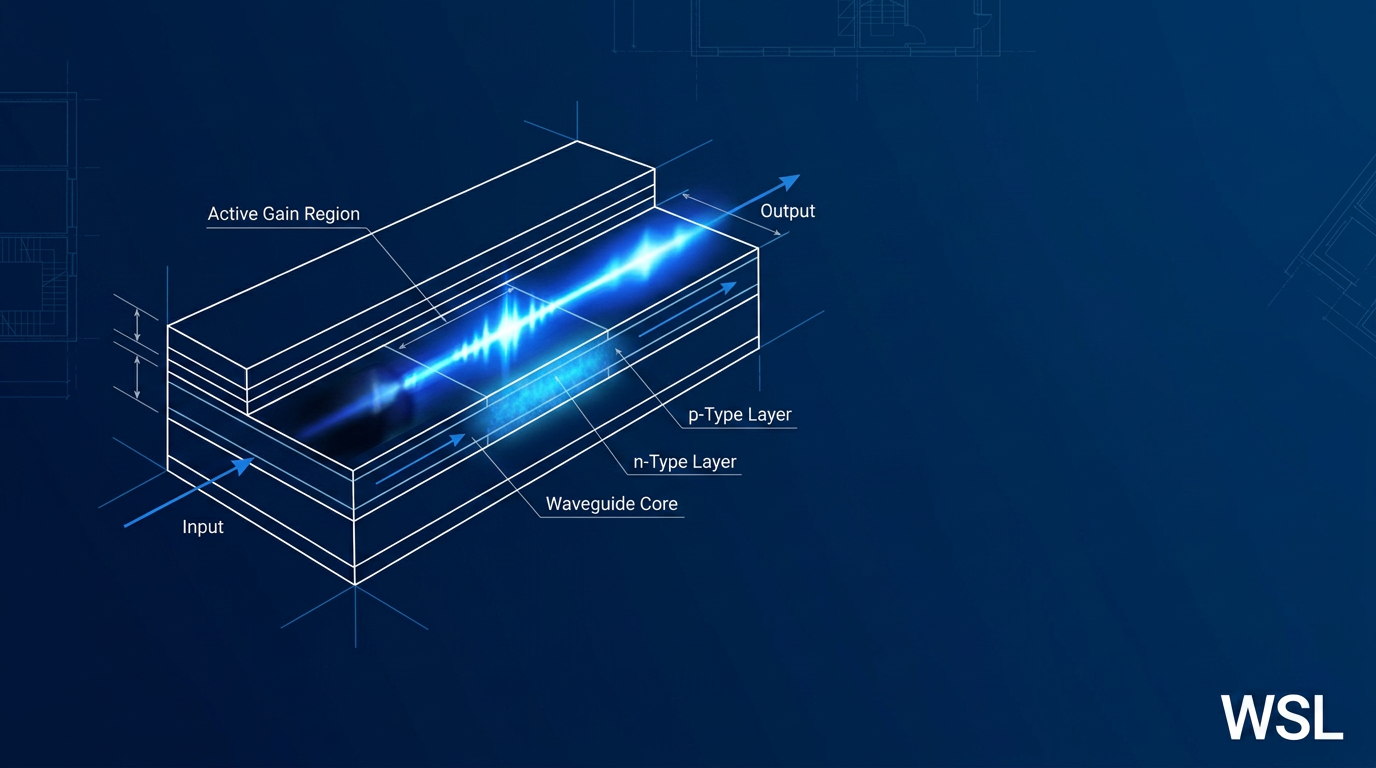
Formally, a semiconductor optical amplifier is a device that amplifies optical signals through stimulated emission in an electrically pumped semiconductor gain medium — a forward-biased p-n junction in which injected current creates the population inversion needed to produce optical gain.
Structure: How an SOA Differs from a Laser Diode
An SOA shares its fundamental architecture with a Fabry-Pérot laser diode: the same semiconductor gain medium, the same waveguide structure, and the same electrical pumping mechanism.
The critical distinction lies not in the gain physics but in what has been done to suppress lasing: antireflection coatings on the facets, angled facets, or a combination of both are used to reduce residual facet reflectivity to the point where the device operates as a single-pass amplifier rather than an oscillator.
An SOA does not use a fundamentally different gain mechanism from a laser diode — it uses the same stimulated emission in the same semiconductor material. The innovation is the suppression of lasing itself: by reducing facet reflectivity sufficiently, the device amplifies light in a single pass rather than building up oscillation.
The active region at the heart of an SOA is typically built from a direct bandgap semiconductor material — InP-based alloys (such as InGaAsP) for telecommunications wavelengths, or GaAs-based materials for shorter wavelengths — with quantum wells or quantum dots commonly used as the gain medium to improve confinement and performance.
Passive waveguide sections at the input and output facets guide light into and out of the active region, completing a compact, chip-scale structure whose total footprint is measured in millimetres.
SOAs in the Optical Amplifier Landscape
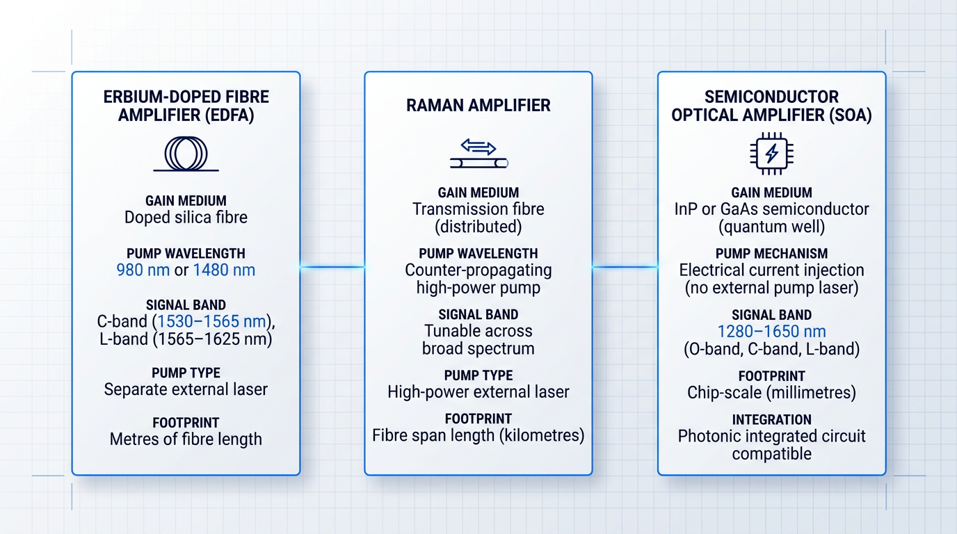
Three principal classes of optical amplifier are used in telecommunications and related fields: erbium-doped fibre amplifiers (EDFAs), Raman amplifiers, and semiconductor optical amplifiers (SOAs).
EDFAs are the dominant amplifier type in long-haul and metropolitan optical networks, using pump light at 980 nm or 1480 nm to excite erbium ions in a doped silica fibre, producing gain in the C-band (approximately 1530–1565 nm) and L-band (1565–1625 nm).
Raman amplifiers achieve gain through stimulated Raman scattering in the transmission fibre itself, with a high-power pump laser launched counter-propagating into the span — a distributed approach that improves signal-to-noise ratio but requires substantial pump power and fibre length.
SOAs occupy a distinct position in this family: they are the electrically pumped, semiconductor-based member, requiring no separate pump laser, fabricated on a chip, and compatible with photonic integrated circuits in a way that fibre-based amplifiers are not.
The absence of a pump laser is a differentiator worth noting early: it has direct implications for compactness, cost, and integration suitability — trade-offs that will be examined in detail when SOAs are compared against EDFAs later in this guide.
SOA technology developed in close parallel with laser diode technology, with early work in the 1960s and 1970s establishing the semiconductor gain medium foundations that both device types share. The pivotal step for practical telecommunications use was the transition from Fabry-Pérot SOAs — which exhibited gain ripple arising from residual facet reflectivity — to travelling-wave SOAs with antireflection-coated facets, which eliminated that ripple and enabled the flat, broadband gain profiles that fibre networks require.
In terms of wavelength coverage, SOAs offer considerable flexibility: by selecting the appropriate semiconductor material composition, they can operate across a broad range spanning roughly 1280–1650 nm, covering the O-band, C-band, and L-band — a span that fibre amplifiers constrained by erbium's atomic transitions cannot match.
This wavelength flexibility, combined with chip-scale integration, positions SOAs across a wide range of application domains including telecommunications, optical signal processing, sensing, and photonic integrated circuits.
With the SOA's basic architecture and position in the amplifier landscape established, the natural next question is how it actually produces gain — the carrier dynamics, stimulated emission mechanics, and rate equations that govern its behaviour, which are the subject of the next section.
How SOAs Work: Physics and Carrier Dynamics
Gain in a semiconductor optical amplifier is not a black box — it follows directly from well-understood quantum mechanics and carrier physics. Build up the picture from first principles and you gain not just an understanding of how gain is produced, but an intuition for why it saturates, why it recovers at the speed it does, and how active region design choices ripple through into system-level behaviour.
The fundamental mechanism is stimulated emission: an incoming photon interacts with an electron sitting in the conduction band and triggers that electron to recombine with a hole in the valence band, releasing a second photon in the process.
Critically, the emitted photon is coherent with the incoming one — identical in phase, frequency, and direction of propagation — which is what makes the process amplifying rather than merely scattering. This stands in sharp contrast to spontaneous emission, where an electron recombines randomly, emitting a photon in an arbitrary direction with no phase relationship to the signal: spontaneous emission contributes noise, not gain.
As the signal propagates along the active region, each stimulated emission event produces a new coherent photon that can itself trigger further events — the result is exponential growth in photon number along the device length, which is the origin of optical gain.
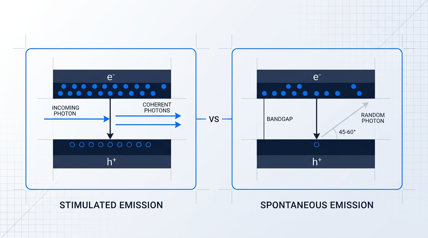
For stimulated emission to outpace absorption, the semiconductor must be in a state of population inversion: more electrons occupying the upper energy states (conduction band) than the lower states (valence band) for the relevant photon energies.
In an SOA, population inversion is achieved electrically. Injecting current pumps electrons into the conduction band and simultaneously creates holes in the valence band — at low injection levels the material is absorbing, but as current increases there is a threshold at which stimulated emission begins to dominate, and the device transitions from absorber to amplifier.
The boundary between these two regimes is defined by the transparency carrier density, N₀: the specific carrier density at which stimulated emission and absorption exactly cancel, leaving the material neither gaining nor losing signal power.
Below N₀ the device absorbs; above it, net amplification occurs. This threshold is a foundational concept for SOA design — the operating current must push the carrier density comfortably above N₀ to deliver useful gain, and any process that depletes carriers back toward N₀ will compress that gain.
The relationship between carrier density and optical gain is captured in the linearised material gain expression: g₀ = Γa(Nc − N₀), where each term carries distinct physical meaning.
- Γ — confinement factor: The fraction of the optical mode overlapping the active gain region. Set by waveguide geometry; typically 0.1–0.4 for quantum-well designs. Higher Γ means more of the signal sees gain.
- a — differential gain coefficient: A material property describing how steeply gain rises with carrier density above transparency. Larger a means more gain per additional carrier injected.
- Nc — carrier density: The actual electron-hole pair density in the active region, controlled by the injection current. This is the quantity the rate equation governs.
- N₀ — transparency carrier density: The threshold density below which absorption dominates. The term (Nc − N₀) is the net inversion above transparency — the effective driving force for gain.
This expression is a linearisation, valid in the vicinity of the operating point — the true gain curve is nonlinear across a wide carrier density range — but it is the form most widely used in SOA design and analysis because it captures the dominant behaviour with tractable algebra.
To understand how carrier density evolves in time — and therefore how gain responds to changing signal conditions — the essential tool is the carrier rate equation: dNc/dt = I/qV − Nc/τs − Rst.
Reading the three terms on the right: I/qV is the rate at which current injection supplies carriers (current I, electron charge q, active volume V); Nc/τs is the rate at which carriers are lost to spontaneous recombination; and Rst is the rate at which carriers are consumed by stimulated recombination — that is, by the amplification of the signal itself.
In steady state, dNc/dt = 0, and the carrier density settles at the level where injection exactly balances both recombination channels. When a strong optical signal is present, Rst grows, depleting carriers faster than injection can replenish them — this is the microscopic origin of gain saturation, and it is why the rate equation is the bridge between input signal power and gain compression.
The timescale over which the carrier density recovers after a perturbation is set by the spontaneous carrier lifetime, τs — approximately 1 ns in typical semiconductor gain media.
With τs around 1 ns, gain recovery between successive pulses becomes incomplete at bit rates above roughly 1 Gbit/s. At those rates, the gain seen by a '1' bit depends on the history of preceding bits — this is the pattern effect, and it is a direct consequence of the interband carrier lifetime.
However, τs is not the only relevant timescale — SOAs exhibit a hierarchy of gain recovery processes, each operating on a different timescale and governing a different class of behaviour.
- Intraband processes (fs to ~1 ps): Spectral hole burning and carrier heating cause sub-picosecond gain changes. Recovery requires only carrier thermalisation within the band — no electron-hole recombination needed.
- Interband recovery (10 ps to ~1 ns): Carrier density recovery via injection and recombination. This is the dominant mechanism for pattern effects and cross-gain modulation at telecom bit rates.
The practical division is this: for ultrafast signal processing involving sub-picosecond pulses, intraband dynamics are the relevant physics; for nanosecond-scale pattern effects and gain modulation at standard telecom bit rates, interband carrier density recovery governs the behaviour.
Active region design directly modifies these dynamics, and it is worth signposting two architectures before the full device taxonomy in the next section. Quantum-well (QW) active regions exploit a two-dimensional density of states that raises the differential gain coefficient a and broadens the gain bandwidth relative to bulk semiconductor — which is why QW designs dominate commercial SOAs today.
Quantum-dot (QD) active regions go further: three-dimensional carrier confinement enables sub-picosecond gain recovery through fast intraband thermalisation between dot ground states and the surrounding wetting layer, alongside lower spontaneous emission noise — making QD SOAs the leading candidate for ultrafast signal processing applications.
With this physical foundation in place — stimulated emission, population inversion, the gain expression, and the full hierarchy of carrier dynamics — the next section examines how different SOA device architectures exploit and manage these principles through structural design choices.
SOA Device Types: A Structural Taxonomy
All semiconductor optical amplifiers share the same fundamental operating principle — stimulated emission in a forward-biased semiconductor gain medium — yet the structural choices made around that gain medium produce devices with radically different performance profiles. Facet reflectivity, gain-region geometry, active-region nanostructure, and cavity configuration are not incidental details: each is a design decision with direct consequences for bandwidth, output power, noise, and application suitability.
Understanding the taxonomy is therefore not an academic exercise. An engineer selecting an SOA architecture for a WDM access network faces a different set of constraints than one amplifying femtosecond pulses for a sensing application, and the device landscape reflects that diversity of demand.
Travelling-Wave SOA (TW-SOA)
The travelling-wave SOA is the dominant architecture for telecommunications, and its defining structural feature is the aggressive suppression of facet reflectivity. By combining antireflection coatings — typically titanium oxide/silicon oxide (TiO₂/SiO₂) multilayers — with angled facets of approximately 7°, residual reflectivity is pushed below 10⁻⁴, and in well-optimised devices to around 10⁻⁵.
Suppressing reflectivity to this level eliminates the Fabry-Pérot resonant cavity, so the signal makes a single pass through the gain medium without forming standing waves. The practical consequence is a gain ripple as low as 0.5 dB and an optical bandwidth exceeding 5 THz — approximately 40 nm in the 1550 nm telecommunications window.
This combination of flat gain and broad bandwidth makes the TW-SOA the default choice for single-channel and WDM amplification, optical switching, wavelength conversion, and 2R/3R signal regeneration in metro and long-haul networks. When the brief simply says "SOA for telecom," a TW-SOA is almost invariably what is meant.
Fabry-Pérot SOA (FP-SOA)
The Fabry-Pérot SOA is best understood as the contrast case: it retains the higher residual reflectivity (~10⁻²) that the TW-SOA works so hard to eliminate, and in doing so it preserves a resonant cavity. This is structurally close to the Fabry-Pérot laser diode architecture introduced in §3 — the difference from a laser is that the device is operated below threshold, so lasing is suppressed but the cavity remains active.
The resonant cavity produces pronounced gain ripple of 10–20 dB and restricts usable bandwidth to just 2–10 GHz. For broadband telecom applications, this is a fundamental disqualification: WDM channels cannot be amplified uniformly across the gain spectrum when the response is so strongly wavelength-selective.
Where the FP-SOA remains useful is precisely in contexts that exploit its wavelength selectivity — narrow-band signal processing and certain sensing applications where the resonant response is an asset rather than a liability. Its primary conceptual value in this taxonomy is as a foil: it shows, concretely, what happens when the travelling-wave condition is not met.
Reflective SOA (RSOA)
The reflective SOA (RSOA) introduces a structurally distinct geometry: one facet is antireflection-coated as the optical port, while the rear facet incorporates a high-reflectivity mirror. Light enters through the AR-coated facet, traverses the gain medium, reflects off the rear mirror, and exits from the same facet it entered — achieving a double pass through the gain region within a single compact chip.
The double-pass geometry delivers higher gain per unit device length than a single-pass design, and the single-port configuration simplifies integration by eliminating the need for separate input and output fibre connections. Both factors make the RSOA inherently compact and cost-effective compared with a full TW-SOA in the same application role.
The primary deployment context for the RSOA is WDM-PON access networks, where it functions as a colourless upstream transmitter at each optical network unit (ONU). In this architecture, a continuous-wave seed signal at the assigned wavelength is sent from the central office; the RSOA at the ONU amplifies and modulates the seed, then returns the upstream data on the same wavelength — eliminating the need for wavelength-specific laser sources at each ONU.
One practical constraint of the RSOA is modulation bandwidth, which is typically limited to the range of 0.6–3.2 GHz for conventional devices. Advanced electronic equalisation and multi-level modulation formats have been demonstrated to push effective operating speeds to around 60 Gb/s with a 3.2 GHz modulation bandwidth, and to approximately 100 Gb/s when bandwidth reaches 5.8 GHz — though these figures depend heavily on signal processing at the receiver.
Tapered SOA
The tapered SOA departs from the uniform-width waveguide of conventional designs by widening the gain region from input to output. This geometry serves a specific purpose: as signal power grows along the amplifier, the expanding active area distributes the optical intensity across a larger cross-section, reducing local intensity and maintaining good beam quality despite very high output power.
The result is a device capable of amplifying ultrashort pulses to peak output powers as high as 9 kW, a figure reported in published conference proceedings for pulsed operation regimes. Continuous-wave performance at watt-class levels has also been demonstrated in published SPIE proceedings, with one tapered SOA delivering over 30 dBm (1.2 W) of fibre-coupled output at 1550 nm and a reported noise figure of 5.4 dB.
This makes the tapered SOA a specialist architecture suited to high-peak-power pulsed applications — amplification of mode-locked diode lasers, optical frequency comb sources, and LiDAR transmitters — rather than a general-purpose telecom amplifier. The tapered geometry is an engineering response to the fundamental trade-off between output power and beam quality that constrains conventional ridge-waveguide designs.
Vertical-Cavity SOA
Vertical-cavity SOA geometries represent a distinct architectural branch in which gain is achieved across a short vertical stack rather than along a long lateral waveguide. The optical path length through the gain medium is orders of magnitude shorter than in a TW-SOA, which fundamentally alters the trade-offs between single-pass gain, beam quality, and integration density.
This geometry is included here for completeness — it represents a valid and distinct architectural branch, with integration characteristics that differ substantially from the lateral waveguide devices that dominate current deployment. Dedicated performance benchmarks for vertical-cavity SOA structures remain less established in the open literature than for TW-SOA or RSOA architectures.
Gain-Clamped SOA (GC-SOA)
The gain-clamped SOA (GC-SOA) addresses a specific impairment that emerges when multiple WDM channels share a single amplifier: variations in total input power cause the carrier density — and therefore the gain — to fluctuate, coupling channels together through cross-gain modulation. The GC-SOA's structural response is to incorporate a distributed Bragg reflector (DBR) or distributed feedback (DFB) grating that sustains an internal lasing mode at a wavelength outside the signal band.
This internal lasing mode acts as a reservoir that pins the carrier density: any excess carriers that would otherwise cause gain fluctuations are consumed by stimulated emission at the clamping wavelength, keeping the gain experienced by signal channels stable regardless of input power variations.
Simulation results confirm that the gain-clamping mechanism significantly reduces third-order intermodulation distortion (IMD) compared with conventional SOAs, though the reduction in channel crosstalk is less pronounced.
The trade-off is a gain-compression penalty at the clamping wavelength and some reduction in available signal gain. The GC-SOA is therefore most valuable in multi-channel WDM contexts where gain stability across channels outweighs the modest gain penalty.
The nonlinear effects the GC-SOA is designed to mitigate — including the full mechanics of cross-gain modulation — are treated in depth in §8.
Quantum-Dot SOA (QD-SOA)
The quantum-dot SOA (QD-SOA) represents the most advanced active-region architecture in current use. As established in §4, quantum-dot active regions confine carriers in all three spatial dimensions, producing carrier dynamics that are fundamentally different from bulk or quantum-well designs — and the consequence that matters most for amplifier performance is gain recovery speed.
Experimental measurements of QD-SOA gain recovery times have demonstrated values of 120–140 fs, four to seven times faster than equivalent bulk or quantum-well SOAs. A separate study of multi-stacked QD-SOAs at 1550 nm estimated an effective carrier transition time of approximately 1 ps using femtosecond pump-probe techniques.
Sub-picosecond recovery enables the QD-SOA to amplify signals at speeds where conventional SOAs would impose inter-symbol crosstalk through slow gain dynamics. This makes the QD-SOA particularly well suited to high-speed all-optical signal processing and multi-channel amplification, where each channel's transient must not perturb the gain experienced by adjacent channels.
The performance parameters that quantify this advantage — including noise figure and saturation output power — are examined in §6, and the signal processing applications that exploit it are developed in §10.
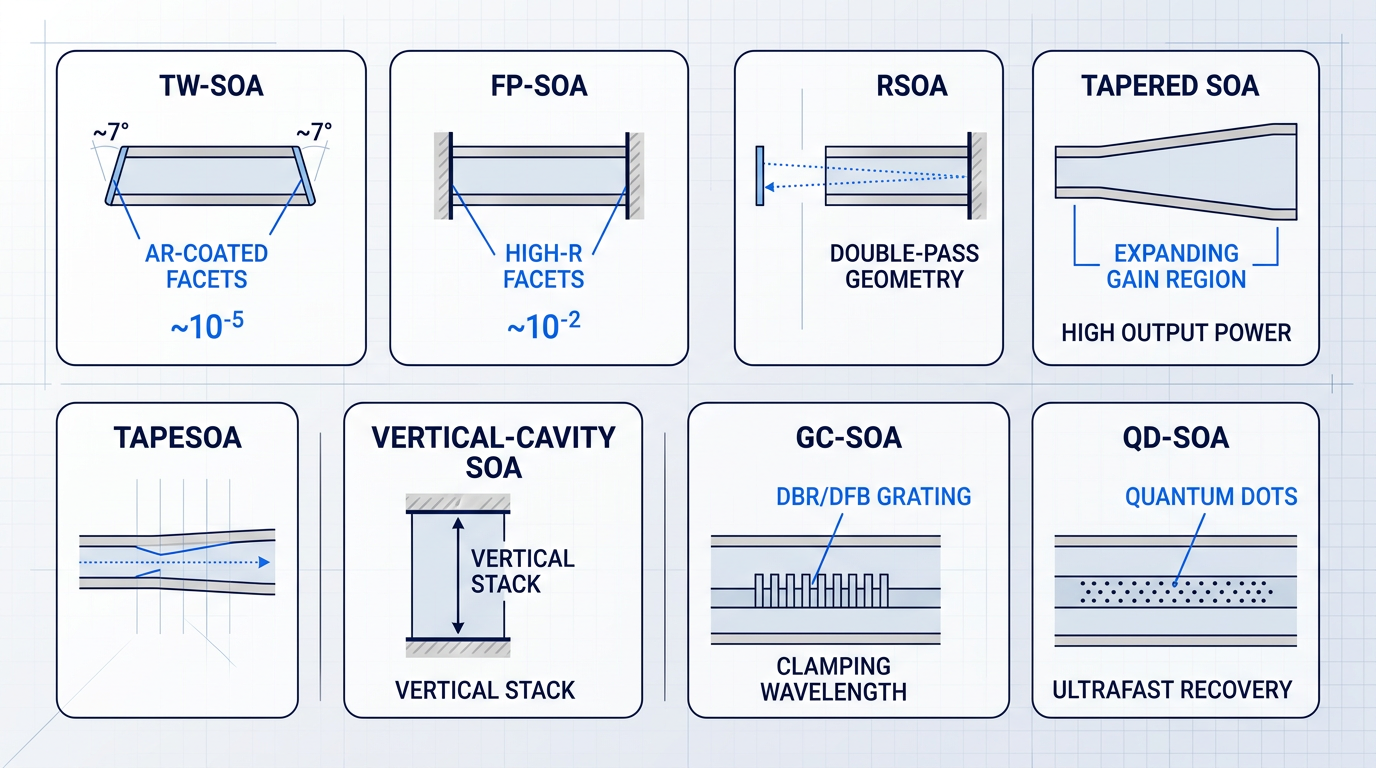
The table below places all seven architectures side by side across the key structural and performance axes, making the trade-offs explicit.
| Device Type | Facet Reflectivity | Bandwidth | Primary Application |
|---|---|---|---|
| Travelling-Wave SOA (TW-SOA) | <10⁻⁴ (down to ~10⁻⁵) | >5 THz (~40 nm at 1550 nm) | Broadband telecom: WDM amplification, switching, 2R/3R regeneration |
| Fabry-Pérot SOA (FP-SOA) | ~10⁻² | 2–10 GHz | Narrow-band amplification, sensing |
| Reflective SOA (RSOA) | <10⁻⁴ (AR facet); high-R rear mirror | 0.6–3.2 GHz (modulation BW) | WDM-PON colourless upstream transmitter |
| Tapered SOA | <10⁻⁴ (AR coated) | Broadband; geometry-dependent | High-peak-power pulsed amplification, LiDAR |
| Vertical-Cavity SOA | Vertical-stack mirrors | Short gain path; geometry-dependent | Compact co-integration; emerging architecture |
| Gain-Clamped SOA (GC-SOA) | <10⁻⁴ (signal facets); DBR/DFB grating internal | Signal band (grating-defined) | Multi-channel WDM; reduced cross-gain modulation |
| Quantum-Dot SOA (QD-SOA) | <10⁻⁴ | Broadband (QD inhomogeneous broadening) | High-speed all-optical signal processing, multi-channel amplification |
Comparison of seven SOA device types across facet reflectivity, bandwidth, and primary application to make architectural trade-offs explicit.
The table makes one pattern immediately apparent: the TW-SOA and QD-SOA share the same low-reflectivity facet requirement but diverge sharply in their active-region architecture — the former optimises for broad flat gain, the latter for ultrafast carrier dynamics. The RSOA occupies a distinct niche defined not by bandwidth but by geometry: its double-pass, single-port configuration is what makes it cost-effective for access networks, not any advantage in raw amplification bandwidth.
The FP-SOA sits apart from all others as the only architecture where higher reflectivity is an accepted feature rather than an engineering failure to be corrected — a useful reminder that the "right" design depends entirely on what the application demands.
The single most consistent thread running through the SOA taxonomy is the relationship between facet reflectivity and usable bandwidth. At 10⁻², a Fabry-Perot cavity forms and bandwidth collapses to 2–10 GHz. Below 10⁻⁴, the cavity disappears and bandwidth opens to beyond 5 THz. Every broadband SOA architecture — TW, RSOA, tapered, QD — depends on achieving and maintaining this reflectivity threshold.
With the device landscape mapped, the natural next question is how to quantify performance across these architectures. Knowing that a TW-SOA offers broader bandwidth than a GC-SOA is useful context; knowing how gain, noise figure, and saturation output power are defined, measured, and compared across device types is what enables engineering decisions. That is the subject of §6.
Key Performance Parameters: Gain, Noise Figure, and Saturation
Reading a single gain figure off a datasheet tells you surprisingly little about whether a semiconductor optical amplifier will actually work in your system — because gain, bandwidth, saturation power, and noise figure interact, and each imposes its own constraint on what the device can do.
Gain: Definition and Driving Factors
Gain is defined as the ratio of output optical power to input optical power: G = Pout/Pin.
In the small-signal regime — where input power is well below the saturation threshold — this gain takes the form G0 = exp(g0L), where g0 is the material gain coefficient and L is the active region length.
The material gain coefficient g0 is not a fixed device constant: it is a function of carrier density, which is itself set by the injection current supplied to the device, as established in the operating principles covered earlier in this guide.
This means gain is an operating-point property — it rises with injection current and falls as input power increases toward saturation.
Practical SOAs can achieve 20–30 dB fibre-to-fibre gain at drive currents around 100 mA, with net gain as high as 30 dB reported for optimised travelling-wave designs.
Engineers reading datasheets should note that fibre-to-fibre gain is always lower than internal chip gain, because coupling losses at the input and output facets — typically up to 3 dB per facet for well-designed tapered waveguide interfaces — subtract directly from the end-to-end signal figure.
Gain Bandwidth
Two distinct bandwidth concepts matter here: material gain bandwidth, set by the semiconductor band structure and representing the full spectral range over which stimulated emission is physically possible, and optical gain bandwidth, the narrower window over which the device delivers net usable gain above a practical threshold.
There is an inherent inverse relationship between peak gain and optical gain bandwidth: operating conditions that maximise gain at a single wavelength tend to narrow the usable spectral window, while designs optimised for broad bandwidth sacrifice some peak gain.
Active region geometry has a direct bearing on this trade-off: quantum-well active regions extend the optical gain bandwidth to 60 nm or more, compared with roughly 45 nm for bulk active region designs operating in the 1550 nm window.
Measured devices confirm this range in practice — commercial SOA arrays have demonstrated greater than 10 dB fibre-to-fibre gain across a 60 nm bandwidth centred at 1550 nm, and purpose-built broadband designs have achieved 3 dB gain bandwidths exceeding 80–107 nm.
Saturation Output Power
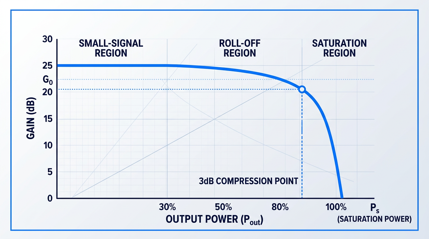
Saturation output power (Psat) is defined as the output power level at which the small-signal gain is compressed by 3 dB — the point at which the amplifier begins to depart from linear operation.
It is governed by the expression Psat = A·Isat,out/Γ, where A is the active region cross-sectional area, Isat,out is the saturation output intensity, and Γ is the optical confinement factor.
The engineering insight encoded in this expression is a genuine design lever: reducing Γ raises Psat, but since gain itself scales with Γ, doing so comes at the direct cost of lower small-signal gain.
Published device data illustrates this trade-off concretely — a higher-confinement quantum-well design delivers up to 23 dB small-signal gain with an on-chip saturation power of 9.2 mW, while a lower-confinement variant of the same design yields 17 dB gain and 15 mW saturation power.
For most commercial SOA applications, achieving output power levels substantially above 10 mW is genuinely constrained by saturation effects — a real limitation that system designers must account for when allocating gain and power budgets.
Noise Figure and Amplified Spontaneous Emission
Noise figure is not a secondary specification — it is one of the two or three parameters that most often determines whether an SOA is viable for a given application.
It is defined as the ratio of input signal-to-noise ratio to output signal-to-noise ratio, expressed in dB: a noise figure of 0 dB would mean the amplifier introduces no degradation whatsoever, which is physically impossible.
Commercial SOAs carry a noise figure in the range of 5–8 dB — a figure that system designers must carry forward in any link budget calculation.
The physical floor on noise figure is set by the spontaneous emission factor nsp (also called the population inversion factor), which quantifies how completely the gain medium is inverted between its energy states.
A perfectly inverted gain medium would have nsp = 1, corresponding to a minimum noise figure of 3 dB — the quantum limit set by the fundamental statistics of photon emission.
Real SOAs operate with nsp greater than 1 because inversion is never complete: residual absorption, internal waveguide losses, and the finite transparency current all mean that some fraction of the carrier population remains in the ground state, generating spontaneous emission that cannot be eliminated.
The noise figure expression Fn = 2nsp(G−1)/G makes this explicit: for high gain, Fn approaches 2nsp, so even a modest elevation of nsp above unity pushes the noise figure well above the 3 dB quantum floor.
The physical mechanism behind this noise degradation is amplified spontaneous emission (ASE): spontaneous recombination events produce photons across the gain bandwidth that are subsequently amplified alongside the signal, creating a broadband noise floor that cannot be filtered away without also cutting signal bandwidth.
The ASE power is described by PASE = nsp(G−1)hfB0, where h is Planck's constant, f is the optical carrier frequency, and B0 is the optical bandwidth over which ASE is collected.
This expression carries three important physical messages: ASE power grows with gain (a higher-gain amplifier produces proportionally more ASE), scales linearly with optical bandwidth (wider filters admit more noise), and is fundamentally bounded from below by nsp.
ASE propagates in both forward and backward directions through the gain medium, so system designs must manage it through optical filtering and careful gain allocation — it cannot simply be ignored at the link level.
In a cascaded amplifier chain, the noise figure consequences compound across stages in a way governed by the Friis formula: the first stage dominates the overall noise performance, but every subsequent stage contributes an additional noise penalty that scales inversely with the gain of the preceding stage.
The practical consequence is that even a modest per-stage noise figure disadvantage accumulates significantly across multiple amplification spans, making noise figure a first-order engineering concern in any multi-stage system design.
In a cascaded amplifier chain, noise figure does not simply add — it compounds. The Friis formula ensures that the first stage sets the noise floor and every subsequent stage worsens it. This is why noise figure must be treated as a primary selection criterion from the outset of system design, not a specification to revisit after gain and bandwidth have been optimised.
Two further practical constraints complete the parameter picture: the output power ceiling imposed by saturation (achieving levels well above 10 mW requires careful design trade-offs that push against fundamental device limits), and the requirement for temperature stabilisation — typically via a thermoelectric cooler — to maintain gain stability as the semiconductor band structure and carrier distributions shift with temperature.
The saturation output power treated here as a static specification is, however, only part of the story — at high input powers, gain compression becomes a dynamic phenomenon that reshapes signal waveforms and opens the door to nonlinear crosstalk effects, which the next section examines in depth.
Polarisation Sensitivity in SOAs: Physics, Impact, and Mitigation
Every semiconductor optical amplifier is, to some degree, polarisation-sensitive — and in a deployed fibre system, where the incoming polarisation state drifts unpredictably with temperature, mechanical stress, and fibre bends, that sensitivity translates directly into a fluctuating output amplitude.
The root cause is geometric. A typical SOA waveguide has an asymmetric cross-section — taller than it is wide, or vice versa — which means the confinement factor is not the same for both principal polarisation modes: Γ_TE and Γ_TM differ, and because modal gain scales with Γ, the TE mode and TM mode see different gain.
In quantum-well SOAs, this geometric asymmetry is compounded by a material effect: QW selection rules favour the electron–heavy-hole transition, which couples preferentially to the TE polarisation, making TE gain the dominant mode by a wider margin than in bulk devices.
The combined effect is captured by the differential gain expression derived in the literature: ΔG|dB = 4.343 × ((Γ_TE − Γ_TM) · g_m + α_TM − α_TE) · L, where g_m is the material gain, α_TE and α_TM are the internal losses for each mode, and L is the device length.
Reading the expression physically: the first term (Γ_TE − Γ_TM) · g_m captures how confinement factor asymmetry converts material gain into modal gain imbalance, while (α_TM − α_TE) · L captures the additional contribution of differential internal loss accumulated over the device length.
In a quantum-well SOA, the geometric confinement asymmetry and the QW selection-rule preference for TE both push in the same direction — making the TE/TM gain imbalance more pronounced than in a bulk device, and harder to eliminate with geometry alone.
The system-level consequence is concrete: an SOA with significant polarisation-dependent gain amplifies a randomly-polarised fibre input with a randomly-varying gain, producing amplitude fluctuations that raise the bit-error rate in digital transmission links.
The SPIE review of SOA requirements sets a practical benchmark: polarisation sensitivity should be less than 0.5 dB for a device to be considered suitable for use with the random polarisation state of a typical link fibre.
Three Engineering Approaches to Polarisation Mitigation
There is no single universal remedy — the right approach depends on whether the device is a bulk or QW design, and whether the engineer has freedom to modify the gain medium, the waveguide geometry, or only the surrounding system architecture.
- Tensile-strained quantum wells: Tensile strain shifts the valence band, promoting electron–light-hole transitions that couple more strongly to TM, counteracting the TE preference of standard QWs. Alternating tensile and compressive strain QW layers can reduce the TE/TM gain imbalance to below 1 dB, with one reported structure achieving 0.1 dB at 100 mA drive current.
- Near-square waveguide geometry: Making the bulk SOA waveguide cross-section approximately square equalises Γ_TE and Γ_TM, removing the geometric root cause. A near-square active waveguide of approximately 0.4 µm × 0.6 µm can achieve polarisation sensitivity as low as 0.3 dB.
- Polarisation diversity schemes: A polarisation beam splitter separates the input into two orthogonal components, each processed by a separate SOA path (or a double-pass through one SOA with a rotator), then recombined — achieving system-level polarisation independence regardless of the SOA's intrinsic PDG.
Each approach represents a different engineering trade-off: tensile-strained quantum wells address the material anisotropy at source but require precise strain engineering during epitaxial growth; the near-square geometry approach is structurally straightforward for bulk SOAs but cannot resolve the QW selection-rule contribution on its own; polarisation diversity schemes achieve polarisation independence at the system level without requiring a specially engineered gain medium, at the cost of added optical complexity and component count.
One further nuance matters for engineers operating real devices: polarisation sensitivity is not a fixed static property — it depends on the operating point.
Bias current and input signal power both alter carrier density, which in turn affects the gain and the refractive index asymmetry between TE and TM modes; under saturation conditions, polarisation rotation can become significant and operating-point-dependent, meaning even a well-designed low-PDG SOA may exhibit degraded polarisation behaviour at high input powers.
That carrier density dependence connects directly to the subject of the next section: the same dynamics that make polarisation behaviour operating-point-sensitive are also the engine behind gain saturation and the nonlinear effects — cross-gain modulation, cross-phase modulation, and four-wave mixing — that define SOA behaviour under high-signal conditions.
Gain Saturation and Nonlinear Effects in SOAs
Gain saturation is the point at which a semiconductor optical amplifier begins to work against itself — and yet the same physics responsible for that limitation is also the foundation for some of the most powerful signal processing capabilities SOAs offer.
As input power rises toward the saturation output power (established in the performance parameters section), stimulated recombination begins consuming carrier density faster than the bias current can replenish it, compressing the gain.
This relationship is captured by the large-signal gain equation: G = G₀ · exp(−(G−1)·Pout/Ps), where G₀ is the small-signal gain, G is the actual gain at output power Pout, and Ps is the saturation power.
Read physically, the equation tells an engineer that gain does not collapse suddenly — it rolls off gradually as Pout climbs, with the exponential term acting as a compression factor that grows stronger the further output power exceeds Ps.
Homogeneous broadening makes this compression a system-level concern in multi-channel WDM links: because all wavelengths within the gain bandwidth draw on the same shared carrier reservoir, a strong channel at any wavelength depletes that reservoir and reduces gain for every co-propagating channel simultaneously.
This fast, cross-channel interaction is a direct consequence of the sub-nanosecond carrier dynamics in SOAs — a characteristic that distinguishes them from amplifiers whose upper-state lifetimes are orders of magnitude longer and which are therefore insensitive to rapid channel-to-channel power variations.
Nonlinear Effects: XGM, XPM, and FWM
When carrier density is modulated by an intense optical signal, it does not merely compress gain — it couples that modulation onto every other signal sharing the gain medium, giving rise to three distinct nonlinear effects that share carrier density modulation as their common root.
- Cross-Gain Modulation (XGM): A modulated pump depletes carrier density periodically, transferring an inverted intensity pattern onto a co-propagating probe at a different wavelength.
- Cross-Phase Modulation (XPM): Carrier density changes alter the refractive index via the linewidth enhancement factor, imposing phase modulation on co-propagating signals.
- Four-Wave Mixing (FWM): Two signals at frequencies f1 and f2 generate new spectral components at 2f1−f2 and 2f2−f1 through the SOA medium's nonlinear susceptibility.
Cross-gain modulation arises because an intensity-modulated pump signal depletes and replenishes the carrier density in synchrony with its own data pattern, so the gain seen by a probe signal at a different wavelength fluctuates in step — the probe acquires an inverted copy of the pump's bit sequence.
In a multi-channel amplifier, that inversion is unwanted crosstalk; in a signal processing context, it becomes a mechanism for all-optical wavelength conversion, with demonstrated speeds scaling with advances in SOA carrier dynamics.
Cross-phase modulation operates through the linewidth enhancement factor (the α-factor), which couples changes in carrier density directly to changes in the refractive index of the gain medium — so the same carrier fluctuations that drive XGM simultaneously impose phase modulation on co-propagating signals.
This phase coupling makes XPM the operative mechanism in interferometric SOA switching configurations, where the phase shift applied to one arm of a Mach-Zehnder or similar structure is the switching signal itself.
Four-wave mixing is distinct in character: two signals co-propagating at frequencies f₁ and f₂ interact through the third-order nonlinear susceptibility of the SOA medium to generate new frequency components at 2f₁−f₂ and 2f₂−f₁.
Critically, FWM preserves both phase and amplitude information in the converted signal — a property cross-gain modulation cannot offer, since XGM transfers only intensity patterns and inverts them in the process.
That transparency makes FWM the preferred mechanism for converting phase-modulated formats such as DPSK, where an intensity-only transfer would destroy the data.
Pattern effects emerge when the carrier recovery timescale (discussed in the operating principles section) is not short relative to the bit period: incomplete gain recovery between successive pulses means the gain seen by any given pulse depends on the sequence of pulses that preceded it.
As bit rate increases, each pulse arrives before the gain has fully recovered from its predecessor, causing bit-error-rate penalties that grow progressively more severe — a genuine and practically significant limitation for SOAs used as inline amplifiers at high bit rates.
The engineering response to XGM and pattern effects is the gain-clamped SOA (GC-SOA), introduced in the device taxonomy section: its internal lasing mode holds the carrier density at a fixed operating point, substantially suppressing the gain dynamics that drive cross-channel crosstalk.
The carrier density modulation that makes XGM, XPM, and FWM impairments in linear amplification is precisely what makes them functional mechanisms in all-optical signal processing.
The cross-channel behaviour explored here — fast, homogeneously broadened gain saturation driving XGM between WDM channels — is one of the sharpest points of divergence between SOAs and erbium-doped fibre amplifiers, and it is the central axis of the technology comparison that follows.
SOA vs. EDFA: An Honest Engineering Comparison
No amplifier technology is universally optimal — the question is never which is better in the abstract, but which fits what the application actually needs.
The semiconductor optical amplifier and the erbium-doped fibre amplifier (EDFA) are the two dominant amplifier technologies operating in the 1550 nm window, and the choice between them carries real system consequences: for noise budget, link reach, integration architecture, and wavelength coverage.
| Parameter | SOA | EDFA |
|---|---|---|
| Noise figure | 5–8 dB (typical commercial devices) | 4–6 dB (practical devices); theoretical minimum 3 dB |
| Gain | 15–30 dB (commercial devices) | >40 dB achievable; typical small-signal 20–40 dB |
| Saturation output power | ~15–18 dBm (typical) | ≥20 dBm in booster configurations |
| Polarisation behaviour | Polarisation-dependent gain; active mitigation required | Inherently polarisation-insensitive |
| WDM cross-channel behaviour | Cross-gain modulation at nanosecond carrier timescales | Immune: erbium upper-state lifetime ~10 ms suppresses XGM |
| Integration suitability | Chip-scale; integrable on InP or silicon photonics; electrically pumped | Requires doped fibre, pump laser, WDM couplers; chip integration impractical |
| Wavelength range | 1280–1650 nm (O, E, S, C, L bands) by material composition | 1530–1565 nm (C-band); 1565–1625 nm (L-band) |
| Component cost | Low (semiconductor fabrication; no pump laser) | Medium to high (pump laser, WDM couplers, doped fibre) |
Side-by-side comparison of SOA and EDFA across eight key engineering parameters, using specific figures from academic and trade sources.
The table reveals two distinct clusters: EDFAs lead on noise figure, gain, and output power — the axes that govern long-haul link budget and multi-channel fidelity — while SOAs lead on integration density, wavelength flexibility, and component cost.
For a system designer, the practical implication is straightforward: if the application's first-order constraints are noise and power, the EDFA is the natural starting point; if the constraints are form factor, integration, or operation outside the C/L window, the SOA is often the only viable option.
Noise figure is the most consequential axis for multi-span system designers. As established when examining the Friis formula context in the performance parameters section, noise figure compounds across cascaded amplifier stages — a 2–3 dB per-stage disadvantage accumulates to a significant optical signal-to-noise ratio penalty over ten or more spans.
In a ten-span system, an SOA with a 7 dB noise figure versus an EDFA at 5 dB represents a 20 dB accumulated noise penalty — a gap that cannot be recovered by gain adjustment alone and that directly limits achievable link reach or required launch power.
This is not a minor footnote: it is the primary reason EDFAs remain the amplifier of choice for long-haul and metro transmission, where noise accumulation across many spans is the binding design constraint.
The WDM cross-channel behaviour difference is structural rather than incremental. As covered in the gain saturation and nonlinear effects section, SOAs' nanosecond-scale carrier dynamics allow cross-gain modulation to transfer intensity fluctuations from one channel to others at data rates, imposing a real impairment in dense WDM operation.
EDFAs do not exhibit this impairment: erbium's upper-state lifetime of approximately 10 ms means the gain medium cannot respond to individual channel intensity fluctuations at gigabit-per-second data rates, making the EDFA gain effectively static across the channel ensemble — a structural advantage for multi-channel WDM that no SOA design parameter can replicate.
Where Each Technology Fits
The engineering axes above map cleanly onto two application-domain clusters, each dominated by the technology whose physical characteristics best match what the application demands.
- Where EDFAs lead: Long-haul and metro telecom, high-power launched-power applications, and multi-channel WDM where low noise and crosstalk-free amplification are first-order constraints.
- Where SOAs lead: Photonic integration, optical switching and signal processing, short-reach data centre interconnects, LiDAR, sensing, and access networks where compactness and wavelength flexibility matter most.
Each technology leads in its domain precisely because its physics align with the application's binding constraints — not because of any incidental feature advantage.
For applications that fall squarely in the EDFA domain — high-power, low-noise, demanding pulse regimes — the degree of engineering applied to the amplifier itself matters considerably. Woodrow Scientific Limited designs and builds custom EDFAs end-to-end to the application: operating band, output power, pulse regime, cooling, form factor, and control firmware are all configured per project rather than accepted from a fixed catalogue, with pulse energies above 10 mJ and average powers above 100 W at the leading commercially available levels for erbium fibre.
With the SOA–EDFA trade-off mapped, the next section examines the specific application domains where semiconductor optical amplifiers have established their strongest positions — from optical switching and data centre interconnects through to LiDAR and emerging photonic integration platforms.
SOA Applications: Telecom, Signal Processing, and Emerging Uses
The physics, device taxonomy, performance parameters, and trade-offs covered in the preceding sections all converge on a practical question: where does the semiconductor optical amplifier actually earn its place in a real system? The answer spans three distinct domains — telecommunications networks, optical signal processing, and a set of emerging applications where SOA characteristics align particularly well with the engineering constraints of next-generation photonic systems.
Telecommunications: Booster, Inline, and Access Network Roles
SOAs can technically serve all three standard amplifier positions in an optical link: as a booster amplifier at the transmitter output, as an inline amplifier compensating for span losses, and as a preamplifier improving receiver sensitivity.
Position-dependence matters here. In long-haul inline roles, the noise figure and output power constraints discussed in the SOA–EDFA comparison limit SOA competitiveness — EDFA noise performance is simply better suited to multi-span terrestrial links where accumulated amplified spontaneous emission noise is the dominant system impairment.
In metro and access network contexts, the picture changes. Shorter spans, lower power budgets, cost sensitivity, and the need for compact, integrable components all favour SOAs — and these networks represent a large and growing deployment base, not a consolation prize for technology that cannot compete elsewhere.
SOAs are particularly well-matched to burst-mode operation in access networks, where traffic arrives in packets rather than as a continuous stream. The fast carrier recovery dynamics of an SOA — operating on picosecond-to-nanosecond timescales — allow the device to respond dynamically to rapidly varying input power levels, a capability that fibre amplifiers with their millisecond-scale gain dynamics cannot replicate efficiently.
SOAs also find deployment in ring network topologies, where they serve dual roles as amplification and optical switching elements within the same compact device — a multifunctionality that is difficult to achieve with fibre-based amplifier technologies.
The most commercially significant access network application is the use of the reflective SOA (RSOA) in WDM-PON architectures, enabling what is known as colourless upstream transmission.
In a conventional WDM-PON, each optical network unit (ONU) at the subscriber end would require a wavelength-specific laser source — a costly and operationally complex requirement when multiplied across thousands of subscribers. The RSOA eliminates this constraint by acting as a wavelength-agnostic upstream transmitter: the central office sends a continuous-wave seed signal downstream at the designated wavelength, and the RSOA at the ONU amplifies and re-modulates that seed signal with upstream data, returning it to the central office without any wavelength-selective source at the ONU.
What makes the RSOA specifically — rather than a generic SOA — the enabling device here is its reflective single-facet architecture. The loopback configuration means the upstream signal traverses the gain medium twice, providing sufficient gain to overcome the double link loss inherent in the loopback path, while the same facet handles both input and output, simplifying the ONU optical assembly considerably.
Research has demonstrated that RSOA-based WDM-PON systems can support upstream operation at 2.5 Gb/s and above, with ongoing work on equalization and multilevel modulation formats pushing achievable speeds significantly higher as RSOA modulation bandwidth continues to improve.
Optical Signal Processing: Nonlinearities as Functional Assets
In linear amplification, XGM, XPM, and FWM are impairments — mechanisms that degrade signal fidelity and limit the number of channels an SOA can amplify cleanly. In optical signal processing, these same mechanisms become the functional core of the application.
The nonlinear effects that constrain SOA performance in multi-channel linear amplification — XGM, XPM, and FWM — are precisely the mechanisms that make SOAs uniquely capable optical signal processors. The impairment and the function share the same physics.
The signal processing applications enabled by SOA nonlinearities span several distinct functional categories, each grounded in demonstrated experimental or simulation results.
- Optical switching: SOA gain can be switched on and off at nanosecond and sub-nanosecond timescales, enabling their use as optical gate elements in photonic cross-connects and data centre switching fabrics.
- XGM wavelength conversion: An intensity-modulated pump depletes carrier density, imprinting an inverted copy of its data pattern onto a co-propagating probe at a different wavelength — transferring data between wavelength channels within a single device.
- FWM wavelength conversion: Four-wave mixing preserves phase and amplitude transparency, making it suitable for advanced coherent modulation formats where XGM's signal inversion and chirp would degrade performance.
- 2R all-optical regeneration: XGM-based re-amplification and re-shaping can restore degraded signals without optical-to-electrical conversion, demonstrated in both bulk and quantum-dot SOA configurations.
- All-optical logic: XGM and FWM in SOAs enable functional all-optical logic gates — AND, XNOR, and digital comparators — representing active research building blocks for all-optical processing architectures.
The optical switching application deserves particular emphasis because it represents a function that fibre amplifiers fundamentally cannot perform. The erbium upper-state lifetime in an EDFA is typically several milliseconds — a physical constraint that prevents any meaningful gain response on nanosecond timescales. SOA carrier dynamics, by contrast, operate on picosecond-to-nanosecond timescales, enabling demonstrated sub-nanosecond switching with burst-mode data transmission in photonic integrated switching architectures.
For XGM-based wavelength conversion, the practical trade-off is well understood: the converted signal is spectrally inverted and carries chirp from the carrier density modulation, which limits its suitability for phase-sensitive modulation formats. For intensity-modulated signals, however, XGM provides a straightforward and chip-compatible conversion mechanism.
FWM-based wavelength conversion addresses this limitation directly. Because FWM is a coherent parametric process, the converted idler preserves both the amplitude and phase of the original signal, making it compatible with formats such as DPSK and QPSK where phase integrity is essential. The trade-off is that FWM efficiency in SOAs depends on the phase-matching conditions and pump-probe wavelength separation, which constrains the usable conversion bandwidth.
For all-optical regeneration, the XGM mechanism enables 2R regeneration — re-amplification combined with re-shaping of the signal waveform — without any optical-to-electrical conversion. Quantum-dot SOAs, with their ultrafast gain recovery arising from the discrete energy level structure of the QD active region, have been demonstrated in simulation at 160 Gbit/s for XGM-based 2R regeneration, exploiting the large XGM bandwidth that QD gain dynamics enable. 3R regeneration extends this concept by adding retiming and clock recovery, fully restoring the signal's temporal and amplitude integrity.
All-optical logic gates based on XGM and FWM — including AND and XNOR functions, as well as digital comparators — have been demonstrated as functional elements, but should be understood as research-stage building blocks rather than commercially deployed components. The engineering path from demonstrated gate function to a practical all-optical processing system remains an active area of investigation.
Emerging Applications: Data Centres, LiDAR, and PIC Integration
Three emerging application areas are attracting significant engineering attention, each driven by a structural alignment between SOA characteristics and the specific constraints of the target system.
In AI data centre interconnects, the demand for bandwidth density, energy efficiency per bit, and co-packaging density is intensifying rapidly as GPU cluster sizes scale. SOAs are well-positioned for short-reach optical interconnects in this environment: they are electrically pumped (requiring no separate pump laser), compatible with photonic integrated circuit platforms, and capable of simultaneous multichannel amplification in a compact footprint. Demonstrated photonic integrated switching architectures using InP-based SOA arrays have achieved sub-nanosecond optical circuit switching with burst-mode data transmission, providing a concrete path toward energy-efficient, low-latency switching fabrics for post-Moore's Law data centre architectures. This remains an emerging deployment area rather than a mature one, but the structural fit is strong.
For solid-state LiDAR, integrated SOAs on photonic platforms address a fundamental engineering problem in large-scale optical phased arrays (OPAs): insertion loss. As OPA element counts scale up to achieve fine angular resolution and wide field of view, the cumulative insertion loss from waveguide crossings, routing, and coupling elements becomes a primary limiter on detectable range. An integrated SOA placed within the OPA circuit boosts the optical signal at the chip level, recovering this loss without requiring higher off-chip laser power. Demonstrated InP OPA systems with integrated on-chip amplification have achieved over 21 dB of net on-chip gain and output powers sufficient for practical ranging, with silicon photonic MEMS-based LiDAR systems demonstrating 3D imaging at ranges of 5–10 m in chip-scale demonstrations and separate LiDAR architectures achieving ranging beyond 40 m. The integration of amplification directly into the photonic sensing front end is a key enabler for compact, chip-scale LiDAR.
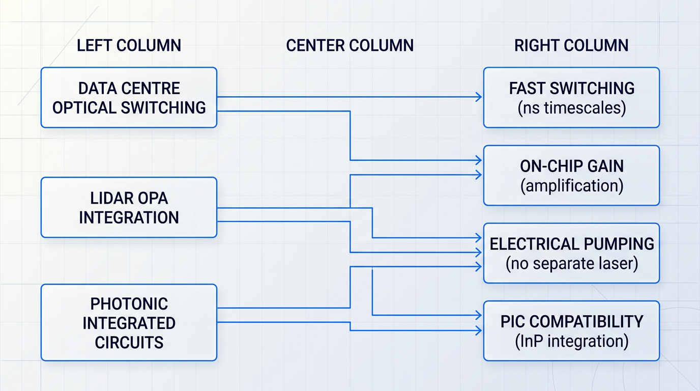
The third emerging context is photonic integrated circuit (PIC) integration itself as an application driver. On InP platforms, SOAs serve as the core active component in complex multi-function chips — enabling chip-scale lasers, amplifiers, modulators, and detectors on a single substrate. The integration advantage is most decisive where the application requires a compact, multi-function photonic subsystem: coherent transceivers, optical phased arrays, photonic neural networks, and high-capacity optical switches all benefit from having gain, modulation, and detection co-integrated rather than assembled from discrete components.
Hybrid III-V/silicon platforms extend this integration capability to silicon photonics manufacturing infrastructure, combining the gain properties of III-V materials with the fabrication scale and CMOS compatibility of silicon — demonstrated with fiber-to-fiber gains exceeding 10 dB and support for advanced modulation formats including QPSK and 16QAM in transmission experiments.
The platform-level detail of how this integration is actually achieved — wafer bonding, heterogeneous integration approaches, and specific InP and silicon photonics fabrication considerations — is the subject of the next section, which examines photonic integration in depth.
Photonic Integration: SOAs on InP and Silicon Photonics Platforms
The most consequential question in next-generation photonic system design is not whether to integrate — it is how. Placing an SOA on a chip alongside lasers, modulators, and photodetectors eliminates inter-component coupling losses and unlocks chip-scale functionality that discrete assemblies simply cannot match, but the path to that integration looks radically different depending on the substrate.
Indium phosphide (InP) is the native platform for SOA integration. As a direct-bandgap III-V semiconductor, InP supports efficient light emission and optical gain without any material import from outside the platform — lasers, SOAs, modulators, and photodetectors can all be fabricated monolithically on a single InP chip, with every optical connection made waveguide-to-waveguide within the same substrate.
That absence of inter-chip coupling loss is a genuine structural advantage, and it has made monolithic InP the dominant platform for complex coherent WDM transceivers deployed in long-haul and metro networks today. The trade-off is wafer scale: InP fabrication typically uses 2-inch wafers, which constrains throughput and keeps per-chip costs high relative to silicon-based alternatives.
Bringing Gain to Silicon Photonics
Silicon photonics offers the economic leverage that InP cannot: fabrication on 200–300 mm wafers at CMOS foundries, with lithographic precision and process maturity built over decades of microelectronics manufacturing. The problem is fundamental — silicon has an indirect bandgap, which prevents efficient radiative recombination, making optical gain essentially impossible in bulk silicon regardless of how the device is engineered.
Any silicon photonic chip that requires optical gain must therefore import III-V gain material from outside the platform. Two mature approaches have emerged for doing this: heterogeneous integration via wafer bonding, and hybrid integration via chip-on-carrier assembly.
In the heterogeneous approach, unstructured III-V epitaxial material — typically InP-based gain layers — is bonded directly onto a silicon-on-insulator (SOI) wafer before device patterning. The bonded III-V film is then processed using CMOS-compatible lithography and etch steps, so the full silicon photonic fab infrastructure can be applied at wafer scale.
Demonstrated devices fabricated this way have shown a maximum fibre-to-fibre gain of 10 dB and a maximum internal gain around 28 ± 2 dB, with transmission performance validated across QPSK, 8QAM, and 16QAM modulation formats over 25 km fibre loops — confirming the approach is not merely a lab curiosity but a viable route for deployed coherent systems.
The hybrid chip-on-carrier approach takes a different philosophy: pre-fabricated SOA die are flip-chip bonded onto a silicon photonic carrier after separate fabrication, rather than co-processed on the same wafer. The critical advantage is yield — only known-good die are assembled, so a defective SOA chip never consumes a finished silicon photonic carrier.
Demonstrated 4-channel SOA arrays assembled via AuSn flip-chip onto SiN photonic carriers have delivered greater than 10 dB fibre-to-fibre gain across a 60 nm bandwidth centred at 1550 nm, with each channel supporting error-free 4-wavelength 25 Gb/s WDM links — a result that directly validates the approach for data centre interconnect use cases.
The choice between wafer bonding and chip-on-carrier is not a question of which is better in the abstract, but which constraints matter most for a given application: wafer bonding offers tighter integration and fab-scale economics at the cost of process compatibility complexity, while chip-on-carrier preserves yield and process independence at the cost of somewhat looser integration.
- Monolithic InP: Native gain platform; zero inter-chip coupling loss; dominant for coherent WDM transceivers. Limited by 2-inch wafer scale and high per-chip cost.
- Heterogeneous (wafer bonding): III-V bonded onto SOI before patterning; CMOS-compatible processing; >10 dB fibre-to-fibre gain demonstrated; 200–300 mm wafer economics.
- Hybrid (chip-on-carrier): Pre-fabricated SOA die flip-chip mounted onto SiN carrier; known-good-die yield advantage; >10 dB gain over 60 nm bandwidth demonstrated.
- 3D Photonic Wire Bonds: Polymer waveguides 3D-printed between InP gain chip and SiP circuit; no precision alignment required; enables >50 nm tuning in hybrid external-cavity lasers.
None of these approaches is universally optimal — the right platform choice is determined by the application's requirements for yield, per-port cost, process compatibility, and integration density, and the field is actively evolving as each approach matures.
The economic argument for silicon photonics integration is straightforward: 200–300 mm silicon wafer processing at CMOS foundries delivers dramatically lower per-chip cost than InP-only fabrication at 2-inch wafer scale, and in data centre interconnect applications where per-port cost is a first-order constraint, that cost differential is the primary commercial driver behind the entire heterogeneous and hybrid integration effort.
One of the clearest demonstrations of what integrated SOAs unlock in practice comes from silicon photonic optical phased arrays (OPAs) for solid-state LiDAR. Large-scale OPAs suffer from 10–20 dB of insertion loss across the array, which historically limited detection ranges to a few metres — insufficient for practical automotive or industrial ranging.
Integrating SOAs directly within the silicon photonic OPA overcomes this loss budget: demonstrated systems have achieved 40-metre range detection and 3D depth scanning up to 20 metres, a result that would not be achievable without on-chip amplification compensating for the array's inherent insertion loss.
A newer integration path is attracting increasing attention: the III-V/SiN platform, where III-V gain material is bonded onto silicon nitride waveguides rather than SOI. SiN waveguides exhibit propagation losses below 0.1 dB/m at telecom wavelengths — orders of magnitude lower than the 2–3 dB/cm typical of SOI strip waveguides — making the platform particularly attractive for narrow-linewidth lasers, sensing, and other applications where ultra-low propagation loss is critical.
The III-V/SiN scheme also requires only a single wafer bonding step to add the III-V layer, compared to the more complex process flows needed for III-V/SOI heterogeneous integration, and SiN wafers carry lower raw material cost than SOI — a combination that positions this platform as an economically attractive path for next-generation integrated photonics.
Silicon photonic fabs process 200–300 mm wafers using infrastructure built for microelectronics. InP fabs typically work at 2-inch wafer scale. That difference in wafer area — roughly 50–100x — is the fundamental economic lever driving heterogeneous and hybrid III-V/Si integration for cost-sensitive applications like data centre interconnects.
With the integration landscape now mapped — from monolithic InP through heterogeneous wafer bonding, hybrid chip-on-carrier assembly, emerging 3D photonic wire bonds, and the III-V/SiN platform — the guide has covered the full SOA technology stack, from fundamental operating principles to the frontier of chip-scale photonic systems. The conclusion draws these threads together into the key engineering take-aways.
Conclusion
Conclusion
The semiconductor optical amplifier is a technology of genuine capability and genuine constraint — and understanding both, with equal clarity, is what makes the difference between a well-matched design and a frustrated one.
The principle this guide has built towards is not a preference for one amplifier technology over another, but a discipline: the right choice is always the one the specific application actually demands, evaluated honestly against noise budget, output power, integration requirements, and wavelength coverage.
Starting from those requirements, rather than from the technology, is where good engineering decisions begin.
Frequently Asked Questions About Semiconductor Optical Amplifiers
Answers to the most common questions about how SOAs work, how they compare to EDFAs, and where they are used.
Commercial semiconductor optical amplifiers typically achieve 15–25 dB fibre-to-fibre gain; optimised designs can reach 30 dB. Fibre-to-fibre gain is the practically relevant figure for system design — it accounts for coupling losses at both input and output facets, so it is lower than the internal chip gain but reflects what the engineer actually sees at the system level. This range is lower than the 20–40+ dB available from erbium-doped fibre amplifiers, but it is entirely sufficient for booster, pre-amplifier, optical gating, and integrated photonic circuit applications. Gain is a function of active region length, carrier density (controlled by drive current), and the optical confinement factor — engineers can trade these parameters against each other to optimise for a specific application without changing the fundamental device architecture.
Gain saturation limits the maximum output power an SOA can deliver, introduces pattern-dependent gain variation at high bit rates, and causes cross-channel gain crosstalk in WDM systems. These three effects are interconnected: all worsen as the SOA is driven closer to or above its saturation output power. Pattern effects arise because the SOA carrier lifetime (typically 100–500 ps) is comparable to the bit period at multi-Gbit/s data rates. When successive mark bits arrive faster than carriers can recover, each pulse sees a different gain level depending on the history of preceding bits — degrading signal quality and setting a practical ceiling on usable bit rate for inline amplification. Cross-gain modulation (XGM) is equally significant in WDM operation: because SOA gain saturation is homogeneously broadened, a strong signal at any wavelength depletes carrier density across the entire gain bandwidth, modulating the gain seen by every co-propagating channel simultaneously. Gain-clamped SOA designs mitigate XGM by using an internal lasing mode to stabilise carrier density, keeping gain approximately constant across a useful range of input powers.
Yes, SOAs can amplify multiple WDM channels simultaneously, but cross-gain modulation (XGM) between channels is a real impairment that must be managed. XGM occurs because the SOA's fast carrier dynamics and homogeneously broadened gain mean that intensity fluctuations in one channel modulate the gain seen by all others — unlike erbium-doped fibre amplifiers, whose upper-state lifetime of around 10 ms causes gain to integrate over millions of bit periods, making interchannel crosstalk negligible in practice. Two mitigation approaches are well established: gain-clamped SOA designs stabilise carrier density via an internal lasing mode, substantially reducing XGM; quantum-dot SOAs benefit from inhomogeneously broadened gain and localised carrier dynamics, which reduce crosstalk and support faster gain recovery. For multi-channel WDM amplification where interchannel crosstalk requirements are stringent, EDFAs remain the preferred technology. SOAs are competitive in access networks and integrated photonic contexts where compactness, electrical pumping, and switching capability matter more than XGM suppression.
SOAs have a higher noise figure than EDFAs primarily because the spontaneous emission factor (nsp) is higher — a consequence of incomplete population inversion and internal waveguide losses. In an ideal amplifier with complete population inversion and zero internal loss, nsp equals 1, corresponding to the quantum-limited noise figure floor of 3 dB. In a real SOA, internal losses from free-carrier absorption and scattering mean that part of the gain medium absorbs rather than amplifies, raising nsp above 1 and pushing the noise figure to 7–12 dB in typical commercial devices. EDFAs can achieve near-complete population inversion with very low internal loss, keeping noise figures in the 4–6 dB range. The practical implication is most acute in cascaded multi-span systems: a noise figure disadvantage per stage compounds across each amplifier in the chain, accumulating into a significant optical signal-to-noise ratio penalty over long distances. In single-amplifier applications — booster, pre-amp, or integrated circuit — the noise figure gap is far less consequential.
SOAs can operate across a broad range from approximately 1280 nm to 1650 nm, covering the O-band, E-band, S-band, C-band, and L-band. The specific operating wavelength is set by the bandgap energy of the semiconductor material in the active region — by choosing different III-V alloy compositions (such as InGaAsP, InGaAs, or InGaAlAs on InP), manufacturers can target different wavelength windows. EDFAs are confined to the C-band (1530–1565 nm) and L-band (1565–1625 nm) by the fixed atomic transitions of erbium ions and cannot be tuned to the O-band or other windows by material choice. This wavelength flexibility makes SOAs particularly attractive for O-band amplification — relevant for short-reach data centre interconnects and access networks — and for applications requiring multi-band coverage on a single chip.
SOAs can switch on nanosecond timescales for optical gating applications — governed by the interband carrier recovery time, which typically falls in the range of 1–10 ns depending on drive current and device design. Quantum-dot SOAs offer significantly faster dynamics: ultrafast intraband relaxation processes (spectral hole burning and carrier heating recovery at ~100–300 fs) enable sub-picosecond gain dynamics, supporting all-optical signal processing at 160 Gbit/s and beyond. In practical terms, nanosecond switching is sufficient for optical packet switching and burst-mode amplification in access networks. Sub-picosecond dynamics are the domain of all-optical wavelength conversion, logic gates, and signal regeneration in high-speed research systems. EDFAs cannot function as optical gates or switches at any practically useful speed — their ~10 ms upper-state lifetime means they respond only to power averaged over millions of bit periods.
A reflective SOA (RSOA) is a single-facet SOA design in which light enters through the front facet, traverses the gain medium, reflects off a high-reflectivity rear mirror, and exits again through the same front facet — giving a double-pass gain configuration in a compact, low-cost package. RSOAs are widely used as colourless upstream transmitters in WDM-PON (wavelength-division multiplexed passive optical network) access networks. In a WDM-PON, each optical network unit (ONU) at the customer premises must transmit on a specific upstream wavelength. A colourless ONU avoids a fixed-wavelength laser entirely: instead, the RSOA modulates and re-amplifies a downstream seed signal injected from the central office at whatever wavelength arrives, allowing a single ONU design to operate at any assigned wavelength. This simplifies inventory and deployment logistics significantly. The double-pass configuration also delivers higher gain than a single-pass SOA of the same chip length — a practical advantage where cost and compactness are primary constraints.
A semiconductor optical amplifier and a laser diode share essentially the same physical structure — an electrically pumped semiconductor gain medium in a waveguide — but the SOA is engineered to suppress lasing and operate as a single-pass amplifier, while the laser diode is designed to sustain optical oscillation. In a laser diode, two cleaved facets form a Fabry–Pérot resonant cavity with reflectivities of around 30%, providing the optical feedback needed for lasing. In a travelling-wave SOA, antireflection coatings and angled facets reduce residual facet reflectivity to below 10⁻⁴, eliminating the resonant cavity — light makes a single pass through the gain medium and exits, amplified but without oscillation. Functionally, a laser diode generates light from electrical input; an SOA amplifies an existing optical signal. The SOA preserves the signal's wavelength, phase, and modulation format within the limits of its noise and nonlinear behaviour — it does not create a new optical signal. This structural similarity is why early SOA development drew heavily on laser diode fabrication technology, contributing to the SOA's relatively low manufacturing cost.