

Introduction
The fibre-optic cable carrying your internet connection and the laser that reshaped someone's cornea this morning have more in common than it might seem.
Both are products of photonics — a field that sits quietly behind some of the most consequential technology in daily life.
Most people encounter it constantly without ever knowing its name: in the LiDAR guiding a self-driving car, the retinal scanner at the optician, the barcode reader at the checkout.
That invisibility is not a problem — it is just what happens when a field becomes infrastructure.
This guide is for engineers, students, and curious professionals who want to understand the field properly: its foundations, its subfields, where it is applied, where it is heading, and how someone builds a career within it.
TL;DR
Photonics quietly underpins global communications, modern medicine, precision manufacturing, and the emerging frontiers of quantum and AI computing — and it remains one of the most structurally underappreciated technical fields in the world, with genuine intellectual depth and strong career opportunity for those who look closely.
This article covers:

The definition, scope, and history of photonics
Major subfields: fibre optics, lasers, imaging, and sensing
Applications across telecoms, medicine, and manufacturing
Emerging frontiers: integrated photonics, quantum, and optical computing
Careers and educational pathways into the photonics industry
What Is Photonics?
Photonics is the science and technology of generating, detecting, and manipulating light — where light means photons, the elementary particles of the electromagnetic field.
The field spans both pure science and applied engineering. It is concerned with the full lifecycle of a photon: emission, transmission, modulation, signal processing, switching, amplification, and sensing.
- Emission: Producing photons from a source, whether a laser, LED, or other light-generating device.
- Transmission: Guiding photons through a medium — optical fibre, waveguide, or free space — with minimal loss.
- Modulation: Encoding information onto a light beam by varying its intensity, phase, frequency, or polarisation.
- Amplification: Boosting optical signals directly, without converting them to electrical form first.
- Detection & sensing: Converting photons back into measurable signals, or using light to probe physical and chemical properties.
Together, these operations define a complete photonic system — analogous to the way generation, transmission, and processing define an electronic one.
The word itself derives from the Greek phos, meaning light. The term "photonics" is relatively modern: it emerged in the late 1960s, coined specifically to describe a field whose ambition was to do with photons what electronics had done with electrons.
That etymology matters. Photonics is not simply a rebranding of classical optics. Classical optics — the study of how light propagates, reflects, refracts, and forms images — is largely descriptive and passive. Photonics is active and applied: it uses light as a functional medium for carrying and processing information, energy, and signals.
Photonics grew out of optics and remains a branch of it, but the two fields are not interchangeable. A lens designer working on aberration correction is doing optics; an engineer designing a coherent optical transceiver is doing photonics.
Photonics vs Electronics: Carriers and Consequences
The most practically useful distinction for readers from engineering backgrounds is the one between photonics and electronics: electronics uses electrons as its information carriers; photonics uses photons.
The physical properties of photons produce real engineering consequences. Photons travel at the speed of light, carry no electric charge, and do not interact with one another or with magnetic fields — giving photonic systems natural advantages in bandwidth, propagation speed, and immunity to electromagnetic interference.
Electronics retains its own strengths: nonlinear signal processing, dense logic integration, and mature fabrication infrastructure at the nanometre scale. Neither field is simply superior to the other — they are complementary, and increasingly integrated in the same devices.
Photons offer speed, bandwidth, and freedom from electromagnetic interference; electrons offer nonlinear processing and compact logic. The most capable modern systems increasingly combine both in the same package.
At the centre of the entire field sits the photon itself: the quantum of the electromagnetic field, massless, travelling at the speed of light in a vacuum.
The photon exhibits wave-particle duality — behaving as a wave in phenomena such as interference and diffraction, and as a discrete particle when absorbed or emitted by matter.
This dual nature is not a philosophical curiosity; it is the reason photonics draws simultaneously on wave optics and quantum mechanics. Wave behaviour underpins waveguiding and coherent imaging; particle behaviour underpins photon counting, stimulated emission, and quantum optical effects explored in later sections of this guide.
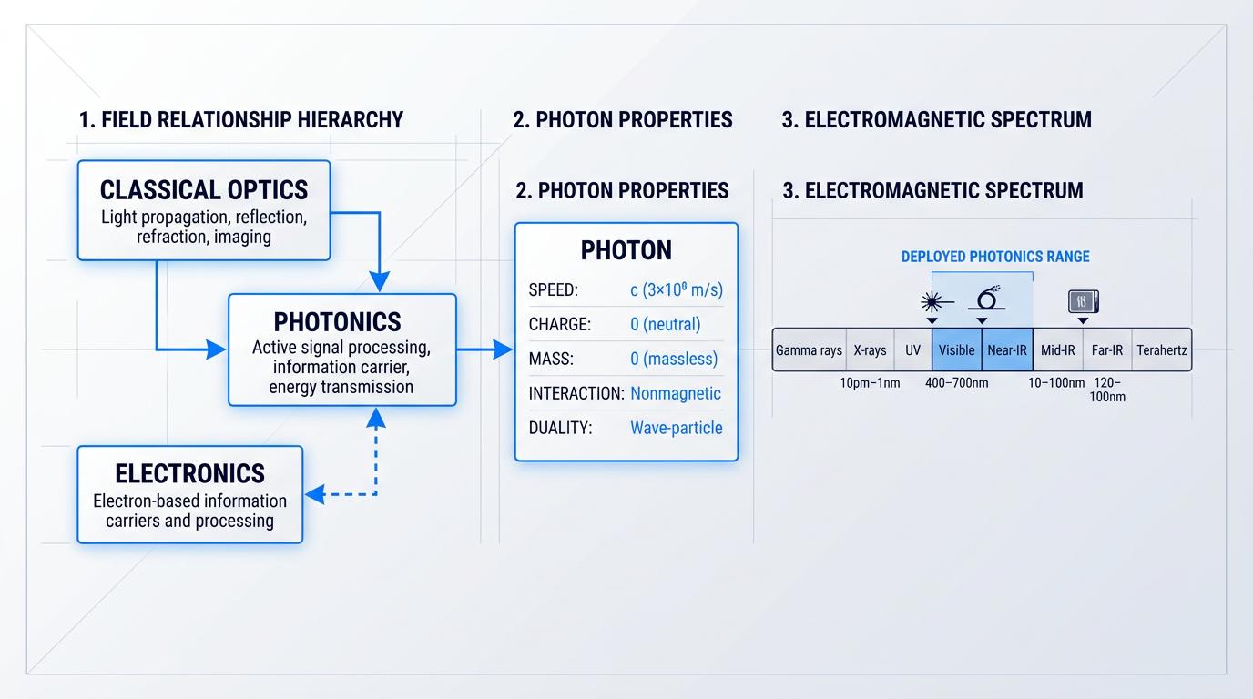
One common misconception is that photonics concerns only visible light. In practice, the field spans the full electromagnetic spectrum relevant to photon-based technologies: from gamma rays and X-rays through ultraviolet and visible wavelengths, into the infrared and out to terahertz frequencies.
The majority of deployed photonic technology operates in the near-infrared to visible range — the wavelengths favoured by fibre-optic communications and most laser systems — but the field's scope extends well beyond what the human eye can detect.
Photonics is also a mature, institutionally organised discipline. The IEEE Photonics Society, SPIE (the international society for optics and photonics), and Optica (formerly the Optical Society of America) collectively structure the field's research publications, engineering standards, and professional community.
Their existence signals something important: photonics is not a niche laboratory curiosity but a well-established discipline with a global community of researchers, engineers, and practitioners.
With the field's definition, scope, and boundaries now in place, the natural next question is how photonics arrived at this point — a story that runs from Newton's prism experiments through Maxwell's equations to the invention of the laser and beyond.
A Brief History of Photonics: To the Laser Age
For centuries, scientists could not agree on something as fundamental as what light actually is. Isaac Newton argued that light consisted of tiny corpuscles — discrete particles travelling in straight lines. Christiaan Huygens countered that light was a wave, spreading outward like ripples on water.
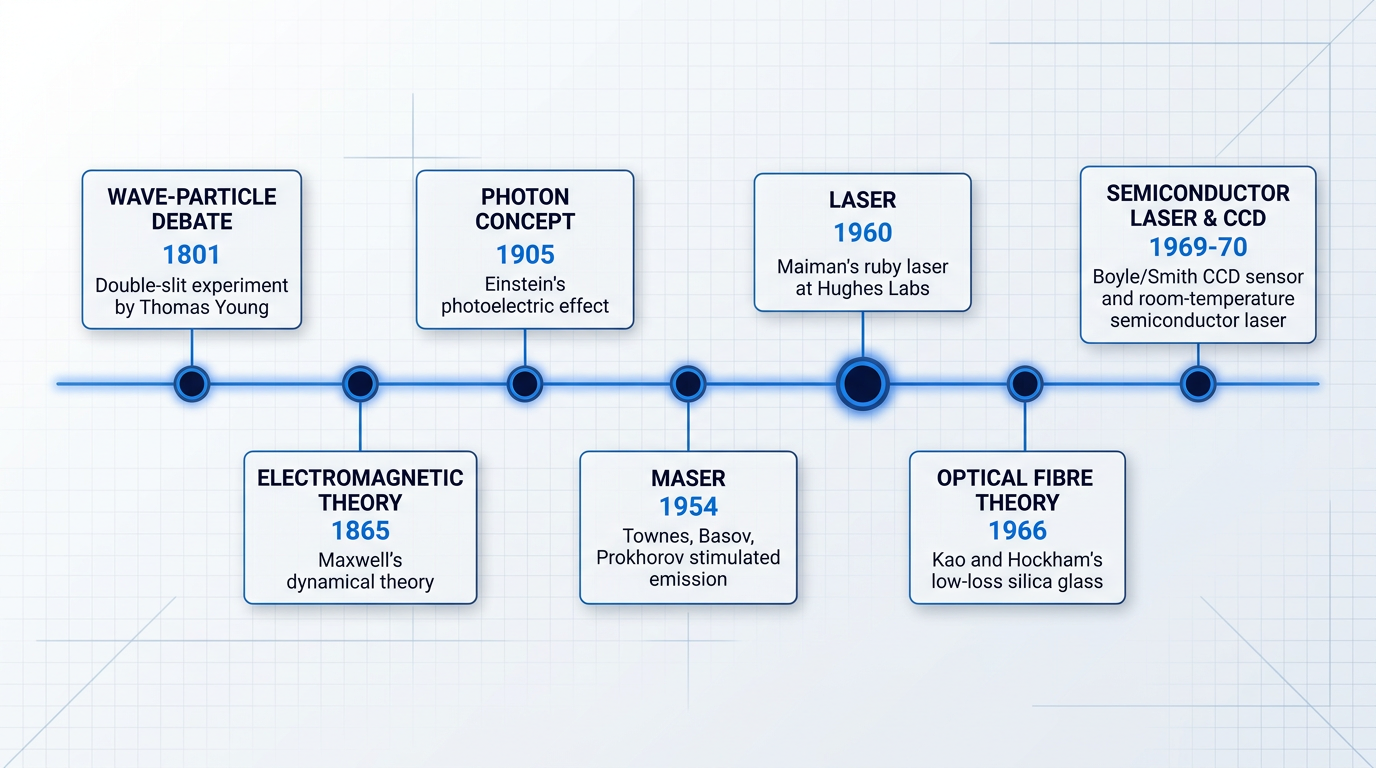
The debate persisted until 1801, when the English physicist Thomas Young devised his now-famous double-slit experiment, shining light through two narrow slits and observing the alternating bands of brightness and darkness that could only be explained by wave interference.
The wave picture was given its deepest theoretical grounding in 1865, when the Scottish physicist James Clerk Maxwell published his dynamical theory of the electromagnetic field, demonstrating that light is a propagating wave of coupled electric and magnetic fields — unifying optics, electricity, and magnetism in a single framework.
Then, in 1905, Albert Einstein ruptured that settled picture entirely. His paper on the photoelectric effect showed that light could only eject electrons from metal surfaces if its energy arrived in discrete packets, not as a continuous wave — a result that demanded light be treated as quantised bundles of energy. Einstein received the Nobel Prize in Physics for this work, awarded for 1921.
It was this concept of the photon — the quantum of light — that opened the door to everything photonics would become. Classical optics described light's behaviour in bulk; the photon concept described how light interacts with matter at the atomic level, making stimulated emission, laser action, and eventually quantum photonics all theoretically conceivable.
The theoretical bridge from Einstein's photon to a practical light-amplifying device was built by Charles Townes, Nicolay Basov, and Aleksandr Prokhorov. Working independently in the early 1950s, they demonstrated that stimulated emission — the process by which an incoming photon triggers an atom to release an identical photon — could be harnessed to amplify microwave radiation.
Their device, the maser (Microwave Amplification by Stimulated Emission of Radiation), first achieved amplification and generation of electromagnetic waves by stimulated emission in early 1954. The Nobel Prize in Physics 1964 was awarded to Townes, Basov, and Prokhorov for this fundamental work in quantum electronics.
The maser was proof of concept. If stimulated emission worked at microwave frequencies, the question was whether it could be achieved at optical frequencies — with visible light rather than radio waves.
On 16 May 1960, Theodore Maiman answered that question at Hughes Research Laboratories in Malibu, California. Using a synthetic ruby crystal pumped by a helical flashlamp, he produced the first working laser — a pulse of coherent red light that no one had achieved before.
Maiman's 1960 ruby laser was not simply a new laboratory instrument. It was the point at which a century of contested physics — from Newton's corpuscles to Einstein's photons — crystallised into an engineering discipline. Within a generation, the laser moved from a curiosity to the backbone of global communications, manufacturing, and medicine.
The field now had a defining technology and, in time, a name to match. The term photonics emerged in the late 1960s — widely credited to the French physicist Pierre Aigrain, though the precise origin remains debated — to describe a discipline that used photons to perform functions traditionally belonging to electronics, particularly in communications and information processing.
Two further milestones cemented photonics as infrastructure rather than laboratory science, and both were recognised with the Nobel Prize in Physics 2009. In 1966, Charles Kao and his colleague George Hockham published a landmark paper arguing that the high optical losses observed in glass fibres were caused by impurities, not by fundamental physical limits — and that sufficiently pure silica glass could carry light over long distances.
That same year, at Bell Laboratories, Willard Boyle and George Smith invented the charge-coupled device — the CCD sensor — in 1969, creating the first practical technology for capturing optical images in digital electronic form and transforming photography, scientific imaging, and eventually consumer electronics.
The infrastructure story accelerated rapidly from there. The first semiconductor laser was demonstrated in 1962, with room-temperature continuous operation achieved by 1970. By the mid-1970s, Corning scientists had fabricated low-loss optical fibres matching Kao's theoretical predictions, and the first optical transmission systems entered service.
Wavelength-division multiplexing — the technique of encoding dozens to hundreds of independent data channels onto a single fibre at different wavelengths — completed the transformation. Optical fibre networks became, as the Nobel committee put it, the circulatory system of the information society.
That trajectory — from a centuries-old argument about the nature of light to the wiring of the internet — is the story of how photonics became a discipline. The laser did not create one application; it seeded an entire family of related fields that together constitute what we now call photonics, and it is those subfields we turn to next.
The Major Subfields of Photonics
Photonics is not a single discipline so much as a family of them — each subfield occupying its own territory, with its own tools, problems, and communities, yet all drawing on the same underlying science of light.
Understanding what each subfield does, and why it exists, is the foundation for making sense of where photonics shows up in the world — and for following the deeper treatments of photonic integrated circuits and quantum photonics that come later in this guide.
Lasers
If photonics has a single enabling technology, it is the laser — the subfield that transformed the field from a theoretical framework into an engineering discipline.
Lasers fall into three broad operating categories: continuous-wave (CW) lasers, which emit a steady, uninterrupted beam; pulsed lasers, which deliver energy in discrete bursts typically ranging from nanoseconds down to around half a nanosecond; and ultrafast lasers, which compress pulses into the picosecond and femtosecond regime.
The distinction between these modes is not merely technical — it determines what a laser can do in practice: CW lasers suit continuous cutting and welding operations, pulsed lasers enable precise material processing with controlled energy delivery, and ultrafast lasers deposit energy so rapidly that surrounding material has no time to heat, enabling micromachining and surgical applications at a precision that other modes cannot match.
Fibre Optics
Fibre optics exploits total internal reflection to guide light along glass or polymer waveguides with remarkably low loss — the physical principle that makes it possible to transmit information as light pulses across thousands of kilometres.
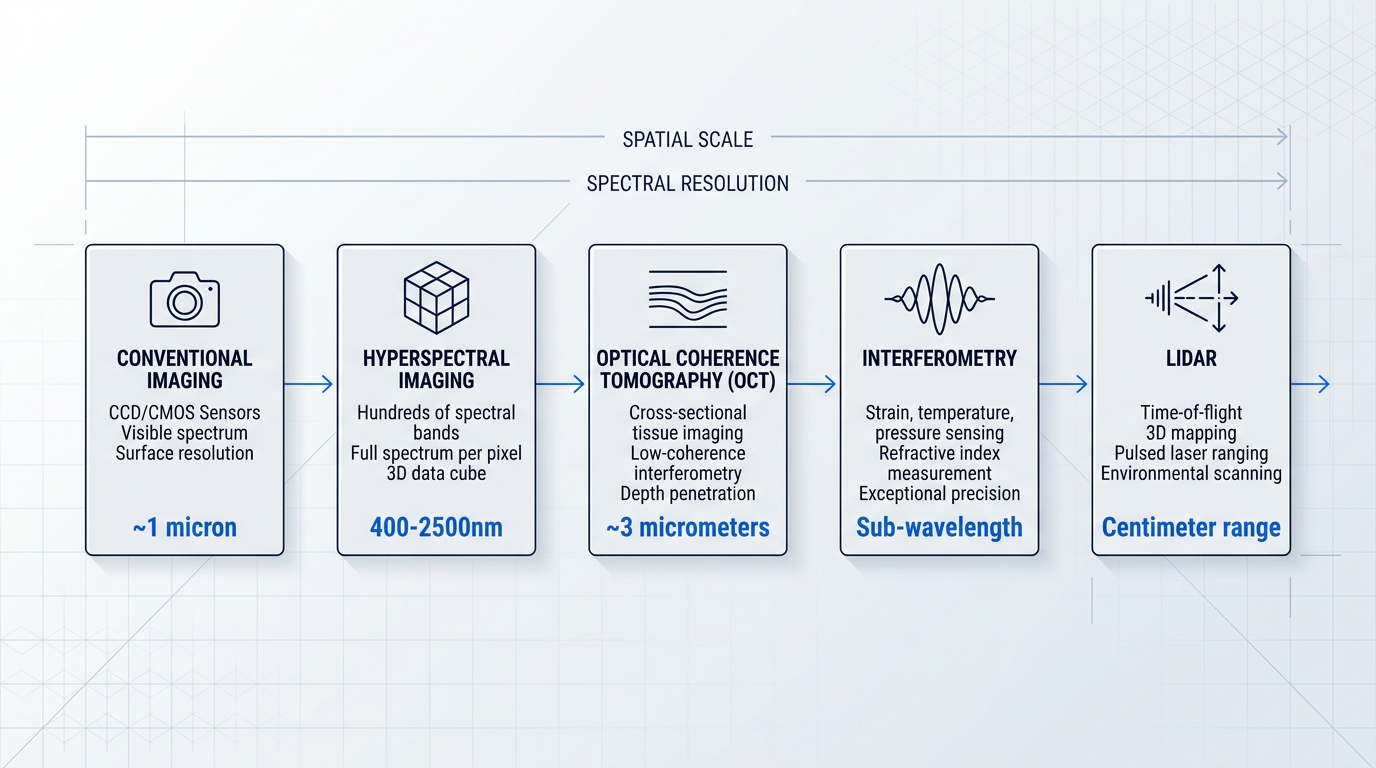
The telecommunications backbone of the modern internet depends on optical fibre, but the subfield extends well beyond data transmission into distributed sensing: techniques based on Brillouin and Raman scattering can map temperature and strain continuously along fibres spanning tens of kilometres, while fibre Bragg gratings (FBGs) — periodic refractive-index structures inscribed into the fibre core — measure strain, temperature, pressure, and vibration at multiple points along a single fibre.
FBG sensors are now embedded in bridges, pipelines, aircraft structures, and wind turbine blades for structural health monitoring, making fibre optics as much a sensing platform as a communications medium.
Imaging and Machine Vision
Photonic imaging is not simply the science of cameras — it is a family of techniques that extend human vision across scales and spectral ranges that the eye cannot reach unaided.
Optical coherence tomography (OCT) uses low-coherence interferometry to produce cross-sectional images of biological tissue with resolutions of a few micrometres, without the need for tissue excision — a capability that has made it the standard of care for retinal imaging in ophthalmology and an established tool for intravascular imaging in cardiology.
Hyperspectral imaging captures hundreds of contiguous, narrow spectral bands simultaneously, producing a three-dimensional data cube in which every spatial pixel carries a full spectrum — enabling material identification and quality assessment in agriculture, food safety, medical diagnosis, and manufacturing inspection at speeds and sensitivities far beyond conventional machine vision.
Optical Sensing and Metrology
Light is an exceptionally sensitive probe: its interaction with matter responds to strain, temperature, pressure, refractive index, and chemical concentration in ways that can be measured with extraordinary precision.
Interferometry, spectroscopy, and distributed fibre sensing all belong to this subfield — each exploiting a different aspect of light's sensitivity to physical parameters to build instruments that out-perform their electronic counterparts in accuracy, speed, or immunity to electromagnetic interference.
The most widely recognised modern example is LiDAR (Light Detection and Ranging), which uses pulsed laser light and time-of-flight measurement to generate precise three-dimensional maps of the surrounding environment — a technology now central to autonomous vehicles and geospatial surveying.
Integrated Photonics
Photonic integrated circuits (PICs) attempt to do for light what the semiconductor industry did for electrons: combine multiple photonic functions — lasers, modulators, waveguides, and detectors — onto a single chip.
The analogy to the electronic integrated circuit is deliberate: just as miniaturising electronics onto silicon unlocked capabilities and economies of scale that discrete components could never match, integrating photonic functions on-chip opens paths to faster, smaller, and more energy-efficient systems for communications, sensing, and computing.
This subfield is treated in depth later in this guide — the introduction here is enough to follow the references ahead.
Quantum Photonics
Quantum photonics marks the frontier where photonics meets quantum information science — moving from treating light as a wave or bulk phenomenon to working with individual photons as carriers of quantum information.
By exploiting the quantum properties of single photons — superposition, entanglement, and the absence of classical noise — this subfield underpins quantum computing, quantum key distribution (QKD) for provably secure communication, and quantum-enhanced sensing.
Like integrated photonics, quantum photonics receives a dedicated treatment later in this guide; the key point here is that it represents photonics operating at its most fundamental level — one photon at a time.
Further Recognised Subfields
The six subfields above are photonics' most commercially mature and broadly active branches, but they do not exhaust the field.
- Nonlinear optics: Studies how high-intensity light interacts with matter to generate new frequencies and enable wavelength conversion, optical switching, and ultrashort pulse generation.
- Photonic metamaterials: Engineers artificially structured materials with optical properties not found in nature, including control over wave propagation in periodically nanostructured and plasmonic systems.
- Terahertz photonics: Covers the generation, detection, and application of electromagnetic waves between roughly 30 GHz and 10 THz — a spectral region with growing uses in imaging and spectroscopy.
- Space photonics: Applies photonic technologies to Earth observation from orbit, space-based optical communications, and the qualification of photonic hardware for the space environment.
Each of these is recognised as a distinct technical group by Optica, the leading international professional society for optics and photonics — a signal that each represents a genuine community of researchers and practitioners, not merely a theoretical category.
Progress in one photonics subfield routinely unlocks capabilities in others: ultrafast lasers enable femtosecond inscription of fibre Bragg gratings; integrated photonics provides the chip-scale light sources and detectors that quantum photonics needs; and LiDAR's advance depends equally on laser, sensing, and PIC developments converging.
With the subfield landscape mapped, the natural next question is where these capabilities land in practice — the industries, instruments, and systems that photonics now underpins.
What Is Photonics Used For?
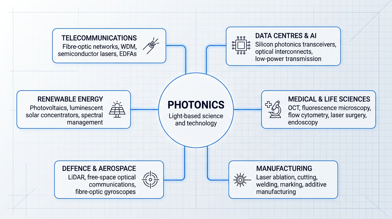
Photonics touches more of the modern economy than most people realise — from the fibre cables carrying internet traffic beneath oceans to the surgical lasers operating inside hospitals, the field underpins industries worth trillions of dollars in aggregate output.
Telecommunications
The global internet runs on glass: fibre-optic networks form the physical backbone of modern telecommunications, carrying data as pulses of light across continents and ocean floors.
Wavelength-division multiplexing (WDM) — and its denser variant, DWDM — multiplies the capacity of a single fibre strand by transmitting dozens to hundreds of independent light channels simultaneously, each at a different wavelength.
Long-haul transmission is sustained by semiconductor lasers as the light sources and erbium-doped fibre amplifiers (EDFAs) to boost signals over thousands of kilometres without converting them back to electrical form.
Telecommunications represents photonics' longest commercial track record and largest installed base — the architecture established over the past four decades now carries the vast majority of the world's data traffic.
Data Centres and AI Infrastructure
Inside modern data centres, optical interconnects are increasingly replacing copper for chip-to-chip and rack-to-rack links, with silicon photonics transceivers among the leading technologies for high-speed intra-facility data transmission.
At the data rates demanded by AI training and inference workloads, photonic links are widely reported to consume considerably less power per bit than their electrical equivalents — a practical advantage already influencing infrastructure design decisions today.
Medical and Life Sciences
Photonics enables clinicians and researchers to see and treat tissue at resolutions and depths that were simply not achievable before coherent light sources and sensitive photon detectors became available.
- Optical Coherence Tomography: Non-invasive cross-sectional imaging of tissue microstructure, used clinically in ophthalmology, cardiology, and oncology.
- Fluorescence Microscopy: Labels specific cellular structures with fluorescent markers, enabling high-resolution imaging in biological research and diagnostics.
- Flow Cytometry: Uses laser light to analyse thousands of cells per second, measuring size, complexity, and fluorescent markers simultaneously.
- Laser Surgery and PDT: Lasers enable precise tissue ablation in surgery; photodynamic therapy uses light-activated agents to destroy tumour cells.
- Fibre-Optic Endoscopy: Flexible fibre bundles transmit illumination and images from inside the body, enabling minimally invasive diagnostic procedures.
Across diagnostics and therapeutics alike, photonics has become a foundational technology layer in modern medicine — not a specialised add-on, but an embedded part of clinical and research workflows.
Manufacturing and Industrial Processing
Industrial laser processing — covering cutting, welding, marking, and additive manufacturing — is a major driver of industrial photonics deployment, with applications spanning automotive, aerospace, electronics, and general fabrication.
Laser ablation is a particularly precise application: the laser's energy couples preferentially to the contaminant or surface layer, selectively vaporising it while leaving the substrate beneath largely intact.
This selectivity makes laser-based surface treatment well suited to demanding cleaning tasks in aerospace component preparation, automotive pre-weld processing, and heritage restoration, where substrate damage is unacceptable.
Woodrow Scientific, the publisher of this guide, manufactures laser cleaning systems that put this physics to work: the ELASER-RHZ uses patented eye-safe technology to collapse the laser hazard zone to a fraction of conventional size, enabling cleaning in open workshops and public-facing environments — such as heritage restoration sites — where standard laser cleaning cannot safely operate.
For high-throughput production environments, Woodrow Scientific's AutoLASE takes a different approach: machine vision scans the loaded part, builds a 3D map, and generates the cleaning path automatically — removing the need for manual programming and making precision laser surface treatment accessible without specialist operator knowledge.
Defence and Aerospace
LiDAR (light detection and ranging) is deployed across military targeting and ranging, civil aviation obstacle detection, and autonomous vehicle navigation — all relying on the same principle of measuring the time-of-flight of laser pulses to build precise spatial maps.
Free-space optical communications provide high-bandwidth, low-intercept data links as an alternative to radio-frequency systems, used in both satellite-to-ground links and tactical communications.
Fibre-optic gyroscopes provide highly accurate inertial navigation for aircraft, missiles, and submarines, as well as structural health monitoring in aerospace platforms.
Directed-energy systems — high-power laser platforms designed to disable or destroy targets — represent an emerging photonic application in defence, with development programmes active across multiple nations.
Renewable Energy
Photovoltaics are, at their core, a photonic technology: the conversion of sunlight to electricity is a photon-electron interaction, with incoming photons exciting electrons across a semiconductor bandgap to generate current.
Luminescent solar concentrators take a photonic engineering approach to improving PV efficiency — fluorescent materials absorb sunlight across a broad spectrum and re-emit it at wavelengths better matched to the cell's absorption band, concentrating usable light without moving parts.
Spectral management — engineering the light spectrum incident on a PV cell to better align with its peak absorption characteristics — is an active research area that applies photonic design principles directly to the efficiency challenge in solar energy.
The breadth of these applications — from submarine cables to surgical suites to solar farms — reflects a field operating at genuine civilisational scale, driving demand for photonic components in volumes that were unimaginable a generation ago.
That demand, in turn, is fuelling one of the field's central engineering challenges: how to integrate the many discrete photonic components required across these domains onto a single chip, at manufacturable cost and scale — the question the next section takes up directly.
Laser Communications Built for Real Infrastructure
Woodrow Scientific develops EDFA technology for free-space optical communications — putting photonics to work where reliable, high-speed data links matter most.

Photonic integrated circuits: the miniaturisation challenge
The semiconductor revolution of the twentieth century was built on a single insight: that discrete components — transistors, resistors, capacitors — could be fabricated together on a single chip, shrinking cost and size while multiplying capability. Photonic integrated circuits (PICs) are attempting the same transformation for light, combining functions that once required a benchtop of discrete optics — light generation, routing, modulation, and detection — onto a substrate no larger than a fingernail.
The component vocabulary of a PIC mirrors its electronic counterpart: waveguides confine and route optical signals on-chip; modulators (typically Mach-Zehnder interferometers or ring resonators) encode data onto light; arrayed waveguide gratings (AWGs) multiplex and demultiplex wavelength channels; and photodetectors convert the optical signal back to an electrical one at the receiver.
The analogy to Moore's Law is instructive but imperfect. PIC integration density has grown steadily — complex InP chips now accommodate more than 1,000 optical components on a single monolithic die — yet the trajectory has been slower than electronics, for reasons rooted in the physics of light itself.
Why miniaturising photonic components is genuinely hard
The fundamental difficulty is that photons are harder to confine than electrons. Optical wavelengths in the near-infrared span hundreds of nanometres to a few micrometres, setting a physical lower bound on waveguide cross-sections and device footprints that has no equivalent in electronics.
Material compatibility compounds the problem. Different photonic functions are optimally performed by different materials — and those materials do not always grow or bond cleanly on the same substrate. Silicon excels as a waveguide medium but is a poor light emitter; indium phosphide emits and amplifies efficiently but guides with higher loss; silicon nitride guides with exceptional low loss but is entirely passive.
The deepest constraint on the dominant platform is silicon's indirect bandgap. In silicon, the conduction band minimum and valence band maximum sit at different crystal momenta, so an electron-hole recombination event must involve a phonon to conserve momentum — a low-probability process that results in an internal quantum efficiency for light emission on the order of 10⁻⁶. This is a fundamental physical property, not an engineering oversight, and it means silicon cannot serve as a laser or optical amplifier without external intervention.
Overcoming it requires heterogeneous integration of III-V compound semiconductors — most commonly indium phosphide-based alloys — onto silicon substrates via wafer bonding or die bonding, adding process complexity and cost to what would otherwise be a straightforward CMOS fabrication flow.
Fibre-to-chip coupling presents a separate engineering challenge. A standard single-mode fibre has a mode field diameter of roughly 10 µm; a silicon waveguide has a cross-section of approximately 0.5 µm × 0.2 µm. The mode mismatch at this interface causes significant insertion loss — typically 1–3 dB per facet in production — even with carefully designed inverse-taper mode converters.
Thermal management becomes critical at high integration density. Silicon's refractive index is temperature-sensitive, so thermal crosstalk between densely packed components can shift ring resonator operating wavelengths and degrade wavelength-division multiplexed channel alignment — a challenge that requires either active thermal control (which consumes power) or athermal device designs (which introduce their own trade-offs).
Manufacturing yield is the final scaling barrier. As the number of components per chip rises, the probability that at least one fabrication defect falls on a critical element rises with it. Yield management at the integration densities the field is targeting remains an active and largely unsolved engineering problem.
The three main PIC material platforms
No single material can serve all photonic functions on a PIC — a fact that has driven the development of three complementary platforms, each with a distinct performance envelope and commercial niche.
Silicon photonics (SOI)
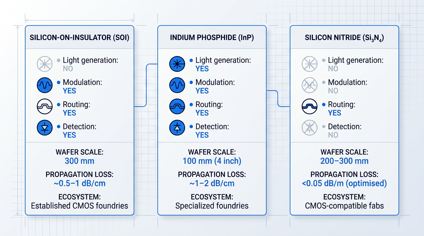
Silicon-on-insulator (SOI) is the dominant high-volume platform. The high refractive-index contrast between the silicon core (~3.45) and the silica cladding (~1.45) enables very compact waveguides, and CMOS-compatible fabrication means PICs can be manufactured in established semiconductor foundries at wafer scales up to 300 mm — giving access to the cost, yield, and process maturity of the mainstream semiconductor industry.
The critical limitation is the indirect bandgap: silicon cannot generate light natively. In practice, the laser source is a separate III-V chip — typically an InP-based continuous-wave DFB laser — that is bonded or butt-coupled to the silicon PIC, with light evanescently coupled into the silicon waveguide layer. This hybrid approach works well for transceivers but adds packaging complexity and cost, particularly when arrays of sources are needed.
Indium phosphide (InP)
Indium phosphide is the only major platform capable of monolithically integrating all four key functions — light generation, amplification, modulation, and detection — on a single material system, because InP is a direct-bandgap semiconductor. This is its defining advantage: a single InP chip can incorporate distributed feedback lasers, semiconductor optical amplifiers, electro-absorption modulators, and photodetectors without any heterogeneous bonding step.
The trade-offs are wafer scale and ecosystem size. InP wafers are typically 100 mm (4 inch) in diameter — SMART Photonics, one of the leading InP foundries, recently scaled from 3-inch to 4-inch production — compared to 300 mm for silicon. Smaller wafer area means higher cost per chip and lower throughput, making InP the preferred platform for high-performance, lower-volume applications such as coherent optical transceivers for long-haul telecommunications.
Silicon nitride (Si₃N₄)
Silicon nitride (Si₃N₄) has emerged as a third platform of growing importance, valued for properties that neither SOI nor InP can match. Its optical propagation loss can reach below 0.05 dB/m in optimised waveguide spirals — among the lowest of any integrated platform — and its transparency window spans from approximately 400 nm in the visible to beyond 2,350 nm in the mid-infrared.
Crucially, Si₃N₄ has no two-photon absorption at telecom wavelengths (unlike silicon), enabling high optical power handling and making it well suited to nonlinear applications such as optical frequency comb generation. Like silicon, it cannot generate light natively — it is a purely passive platform — but its ultralow loss makes it the preferred medium for long delay lines, precision sensing, LiDAR, and quantum photonic circuits where loss is the dominant performance constraint.
| Platform | Native light emission | Typical wafer size | Propagation loss | Primary applications |
|---|---|---|---|---|
| Silicon-on-insulator (SOI) | No — III-V hybrid integration required | 300 mm | ~0.5–1 dB/cm (channel waveguide) | Data centre transceivers, LiDAR, biosensing |
| Indium phosphide (InP) | Yes — direct bandgap, all functions monolithic | 100 mm (4 inch) | ~1–2 dB/cm | Coherent transceivers, long-haul telecom, high-performance PICs |
| Silicon nitride (Si₃N₄) | No — passive platform only | 200–300 mm (CMOS fab) | <0.05 dB/m (optimised spirals) | Sensing, LiDAR, frequency combs, quantum photonics |
Comparison of the three main PIC material platforms across key technical and commercial dimensions, enabling readers to understand the trade-offs that drive platform selection.
The table makes the core trade-off concrete: SOI wins on scale and cost; InP wins on monolithic functional completeness; Si₃N₄ wins on loss and wavelength range. No single platform dominates all use cases, which is why commercial PIC systems — including high-performance coherent transceivers — increasingly combine two platforms in the same module, using InP for the laser source and silicon or silicon nitride for routing and modulation.
The three PIC platforms are complementary by design: SOI provides scale, InP provides active functionality, and Si3N4 provides ultralow loss. The field is converging on heterogeneous integration — combining the strengths of each — rather than on a single universal material.
The commercial deployment picture reflects this maturity. Silicon photonics transceivers operating at 800 Gbit/s are shipping products today, deployed in hyperscale data centres by vendors including Lumentum and Coherent. LightCounting projects silicon photonics chip sales will grow from $0.8 billion in 2023 to over $3 billion by 2029, with SiP transceivers crossing 50% of the total optical transceiver market by value in 2026.
The application domains driving this growth extend well beyond data centre interconnects: LiDAR for autonomous vehicles, photonic computing accelerators, chip-scale biosensors, and integrated quantum photonic circuits are all active areas of PIC development, each placing distinct demands on the underlying platform.
Several engineering challenges remain open. On-chip light sources for silicon — even with heterogeneous bonding — add cost and limit the density of WDM source arrays. Fibre-to-chip coupling loss of 1–3 dB per facet is acceptable for current transceivers but becomes a budget problem in loss-sensitive quantum and sensing applications. Thermal crosstalk on densely integrated chips requires active compensation that itself consumes power. And manufacturing yield at the integration densities the field is targeting has not yet been demonstrated at the scale the most ambitious designs require. These are active engineering problems, not fundamental barriers — but they set the pace of the field.
The integration challenges described here become considerably more demanding when the photons must carry quantum information rather than classical data — where loss is not merely a performance penalty but a source of decoherence, and where single-photon sources and entanglement generation impose requirements that no current platform fully satisfies. That is the terrain of quantum photonics, explored next.
Quantum photonics: light at the edge of what is possible
The fibre-optic cables carrying today's internet traffic operate on classical physics — light as a wave, encoding information in amplitude and phase. Quantum photonics uses those same physical carriers but in an entirely different regime: individual photons, governed by quantum mechanics, capable of doing things no classical signal can.
At this level, photons exhibit two properties that classical light does not. Superposition means a single photon can encode multiple states simultaneously, rather than a fixed 0 or 1. Entanglement means two photons can share a correlated quantum state such that measuring one instantly determines something about the other, regardless of the distance between them.
These are not just curiosities — they are the physical foundation for a new class of technologies in computing, communication, and sensing. But photons have a particular set of properties that make them especially well suited as quantum information carriers, beyond simply being the particles of light.
- Low decoherence: Photons interact weakly with their environment, so quantum states are preserved longer than in many competing approaches, such as superconducting qubits requiring millikelvin cooling.
- Fibre compatibility: Photons already carry global telecommunications traffic, so quantum communication can leverage existing fibre-optic infrastructure without building entirely new networks.
- Room-temperature operation: Many photonic quantum systems operate at or near room temperature, unlike superconducting qubit platforms that require extreme cryogenic environments.
These advantages are genuine physical properties, not marketing claims. The honest counterpoint is that photons also present a real challenge: they do not interact easily with each other, which complicates certain gate operations needed for quantum computing and remains an active area of research.
Quantum computing with light
Linear-optical quantum computing (LOQC) is the photonic approach to quantum computation. It uses single-photon sources, beam splitters, phase shifters, and photon-number-resolving detectors to perform quantum gate operations — the building blocks of computation — using light alone.
Fabricating these components together on a single chip, as integrated quantum photonic chips, enables implementations that are more stable and manufacturable than bulk-optic laboratory setups. Research published in Nature Photonics has documented the progression from few-component circuits to programmable devices approaching 1,000 components on millimetre-scale footprints.
The current state deserves honest framing. Demonstrations of key building blocks — entangled photon pairs, on-chip entanglement generation, small-scale quantum circuits — have been achieved. Large-scale, fault-tolerant photonic quantum computers remain a research challenge, not a near-term commercial product.
Quantum communication and QKD
This is the most commercially mature pillar of quantum photonics. The security foundation is the no-cloning theorem: it is physically impossible to copy an unknown quantum state without disturbing it, which means any attempt to intercept a quantum-encoded message leaves a detectable trace.
Quantum key distribution (QKD) exploits this principle to distribute encryption keys with security rooted in physics rather than computational difficulty. The BB84 protocol — which encodes key information in the quantum states of photons — is the most mature approach and the basis for most deployed QKD systems today, according to the UK Government's QKD research report.
In practice, standard QKD systems operate effectively over approximately 100–200 kilometres of optical fibre before signal degradation becomes prohibitive. To extend distances, trusted-node architectures are used, though these introduce relay points that break end-to-end quantum security.
Satellite QKD extends the range by transmitting quantum states through free space. China's Micius satellite demonstrated entanglement-based QKD between two ground stations separated by 1,120 kilometres, achieving a secret-key rate without trusted relays — a result published in Nature in 2020. In 2017, the same satellite had distributed entangled photon pairs between ground stations separated by 1,203 kilometres, setting a new distance record for quantum entanglement at the time.
Quantum sensing
Quantum sensing exploits the extreme sensitivity of quantum states to physical perturbations. Because quantum systems respond measurably to tiny changes in their environment — a property that makes building quantum computers difficult — that same sensitivity becomes a virtue when precision measurement is the goal.
Atomic clocks are the most familiar example: already the most precise timekeepers in existence, they underpin GPS navigation and telecommunications synchronisation worldwide. Quantum magnetometers detect faint magnetic fields for applications ranging from medical imaging to geological surveying.
Quantum gravimeters measure gravitational anomalies with precision that surpasses classical instruments, enabling underground mapping and navigation applications. Gravitational-wave detection provides perhaps the most dramatic example: LIGO injects squeezed states of light into its interferometers to push measurement sensitivity below the quantum shot-noise limit, a technique confirmed operational since 2019.
According to a 2024 Nature review, quantum gravimeters, magnetometers, and atomic clocks are already commercially available and being evaluated in energy-sector environments. This pillar is not speculative — it is deployed.
QKD networks are commercially deployed and atomic clocks already underpin global infrastructure. Photonic quantum computers at scale remain a research frontier. Both facts are true simultaneously — and conflating them in either direction misrepresents the field.
Scaling all three pillars from laboratory demonstrations to manufacturable systems depends critically on the chip-scale integration covered in the previous section. Fabricating single-photon sources, waveguides, beam splitters, and detectors onto a single photonic chip is the path from proof-of-concept to deployable quantum technology.
Governments have assessed this trajectory and are investing accordingly. The UK National Quantum Strategy commits £2.5 billion over ten years from 2024 to quantum research and innovation. The EU Quantum Flagship programme and the US National Quantum Initiative represent parallel commitments across major economies. Photonics is a central enabling technology across all three programmes.
Quantum photonics represents one frontier where photonics is redefining what information processing can mean at a fundamental level. The next section examines a different but equally consequential frontier: how photonics is reshaping classical computing infrastructure and accelerating the development of AI.
Is Photonics the Future of AI?
AI's appetite for data movement is outpacing what copper can physically deliver — and that gap is where photonics has become not a future aspiration but a present necessity.
Training a large language model requires thousands of GPUs to exchange data continuously, at bandwidths that copper interconnects simply cannot sustain over the distances involved inside a modern data centre.
At 100 Gb/s, copper signals degrade after roughly two metres; at 200 Gb/s, that drops to around 1.5 metres — a hard physical constraint that no amount of engineering refinement will eliminate.
Optical fibre carries vastly more data per second, over distances measured in hundreds of metres rather than centimetres, with lower signal loss and lower energy per bit transmitted.
Optical interconnects: the photonics already powering AI
This is not a forecast — silicon photonics transceivers are already the dominant technology for intra- and inter-data-centre links, and the commercial trajectory is accelerating sharply.
According to LightCounting, 2026 marks the first year in which silicon photonics modulators will account for more than 50% of the total optical transceiver market — up from just 10% in 2018 and 33% in 2024.
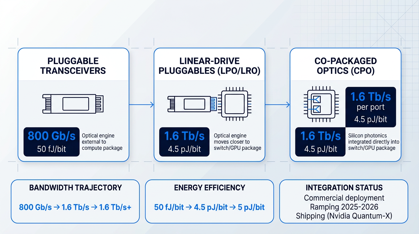
As discussed in the section on photonic integrated circuits, 800 Gb/s silicon PIC transceivers are already in commercial deployment; the industry is now ramping 1.6 Tb/s modules, with 3.2 Tb/s on the roadmap.
The next integration steps go further still: co-packaged optics (CPO) and linear-drive pluggables (LPO/LRO) bring the optical engine physically closer to — or directly onto — the switch or GPU package, cutting the electrical signal path to a minimum.
Nvidia's Quantum-X and Spectrum-X Photonics switches, which integrate silicon photonics directly into the switch package at 1.6 Tb/s per port, illustrate how rapidly CPO is moving from research concept to shipping hardware.
LightCounting projects that CPO and LPO will together double silicon photonics' market share from roughly 30% in 2025 to 60% by 2030, driven primarily by scale-up network applications connecting dense GPU clusters.
The energy efficiency argument
AI training and inference rank among the most energy-intensive computing workloads ever run at scale — and the trajectory is steep: a 2024 report from the US Electric Power Research Institute projected that data centres could consume up to 9% of total US electricity generation by the end of the decade.
Photons do not generate resistive heat losses the way electrons do in copper wiring — a grounded physical advantage that translates directly into lower energy per bit transmitted.
A 3D-integrated photonic transceiver platform reported in Nature Photonics achieved 50 fJ per communicated bit from the transmitter front end — a figure that, at data-centre scale, represents a meaningful reduction in the megawatt-level power budgets that optical modules now represent.
Research modelling published in SPIE proceedings shows that CPO transceivers operating at 106 Gb/s PAM4 can achieve a link energy of 4.5 pJ/bit — well within targets set for energy-efficient AI and ML interconnects.
For shorter on-package distances, optical I/O achieves 4 Tb/s signal transfer with only 5 ns latency and 5 pJ/bit energy consumption, representing roughly 10 times better performance in both speed and energy efficiency compared to electrical I/O at equivalent data rates.
The sustainability dimension matters beyond operational cost: SPIE has highlighted that photonic approaches to data centre efficiency represent one of the clearest paths the photonics industry has toward reducing the sector's growing carbon footprint.
Photonic AI accelerators: the frontier
The interconnect story is settled technology; the photonic AI accelerator story is something different — a rapidly advancing research frontier with demonstrated results, but not yet commercially mature.
The core physical argument is compelling: photonic matrix-vector multiplication operates at sub-nanosecond timescales, because an entire matrix computation can complete in less than a single electronic clock cycle — limited by the propagation time of light through the circuit rather than by transistor switching speeds.
The foundational demonstration came from Shen et al. at MIT, who showed that an optical neural network architecture could achieve at least two orders of magnitude speed improvement over conventional digital computation for forward propagation, with power efficiency scaling linearly rather than quadratically with network size.
More recent work has pushed the scale considerably further: a 2025 Nature paper reported a 64×64 photonic accelerator integrating more than 16,000 photonic components on a single chip, achieving an average bit accuracy of 7.61 bits and demonstrating latency two orders of magnitude lower than electronic alternatives for matrix-vector computation.
A separate 2025 Nature paper presented a photonic AI processor capable of executing advanced models including ResNet and BERT, achieving near-electronic precision for many workloads — described by its authors as a notable entry for photonic computing into competition with established electronic AI accelerators.
On the interconnect side, a 3D-integrated photonic platform reported in Nature Photonics achieved 800 Gb/s aggregate bandwidth from a 0.3 mm² footprint — a density of 5.3 Tb/s per mm² — demonstrating how tightly photonics and electronics can now be co-integrated.
Experimental photonic neural cellular automata have demonstrated 98.0% classification precision at a throughput of 1.3 µs per frame — faster than the same task running on an NVIDIA T4 GPU, even accounting for the GPU's parallelism advantages.
These results are genuine and significant — but they come with important caveats: current photonic accelerators operate at limited numerical precision (typically 4–8 bits), face challenges with programmability and reconfigurability, and have not yet demonstrated the manufacturing yield needed for large-scale commercial deployment.
The barriers are real: thermal stability, device variability across a wafer, the energy cost of analogue-to-digital conversion at the chip boundary, and the difficulty of implementing nonlinear activation functions optically all remain active engineering problems.
Neuromorphic photonics: a longer-horizon frontier
At the furthest edge of this landscape sits neuromorphic photonics — using photonic integrated circuits to implement neural network architectures directly in hardware, operating at timescales that electronics cannot approach.
A foundational review in Nature Photonics (Shastri et al.) established that photonic neuromorphic systems offer sub-nanosecond latencies — a qualitative advantage over electronic neuromorphic approaches, which are constrained by the same resistive and capacitive limits as conventional processors.
VCSEL-based spiking photonic neurons have been demonstrated operating at speeds up to nine orders of magnitude faster than biological neurons and, crucially, up to six orders of magnitude faster than their electronic neuromorphic counterparts — a claim grounded in the fundamental physics of photon propagation versus electron transport.
Demonstrations now include photonic spiking neural networks performing time-series prediction at roughly 120 µW average power, and integrated neuromorphic circuits with on-chip analogue memory showing over 26 times power savings compared to conventional SRAM-DAC architectures for equivalent inference tasks.
This is a field where the physics is unambiguously promising and demonstrations are accumulating — but device variability, the absence of standardised benchmarking metrics, and the challenge of scaling from proof-of-concept chips to manufacturable systems mean neuromorphic photonics remains further from commercial deployment than optical interconnects or even photonic AI accelerators.
Photonics is already essential infrastructure for AI: silicon photonics transceivers handle the data movement that makes large-scale training and inference possible, and this is a present reality, not a future promise. Whether photonic processors displace electronic ones for the computation itself is an open question — experimental demonstrations are advancing rapidly, but general-purpose photonic AI processors have not yet achieved the precision, programmability, and manufacturing yield needed for commercial deployment at scale.
The question "Is photonics the future of AI?" has a two-part answer: for data movement, photonics is already the present; for computation, it is the field's most consequential open frontier.
That combination — deployed at scale in one dimension, advancing rapidly in another — is precisely why photonics is attracting significant research investment and why careers at the intersection of photonics and computing are among the most sought-after in the field, as the next section explores.
EDFA Technology for High-Speed Optical Communications
Woodrow Scientific builds EDFA solutions for free-space optical communications — the photonics infrastructure keeping data centres connected at the speeds AI demands.

Careers in Photonics: Pathways into the Field
Photonics underpins the internet, medical imaging, defence systems, and now AI computing infrastructure — yet it remains one of the least publicly visible technical fields in the world, and that combination is genuinely unusual: strong structural demand, a persistent workforce shortage, and a talent pool that has never kept pace with the industry's growth.
A 2021 workforce study supported by AIM Photonics projected that middle- and lower-skilled positions in the US photonics industry would grow from around 58,000 to nearly 85,000 by the end of the decade — translating to roughly 42,000 cumulative middle-skilled openings over the period, or approximately 3,500 new middle-skilled hires needed every year.
Engineering technicians alone are projected to represent more than 22,500 openings across the decade in the US — at an average hiring rate of 2,200 per year. The same study estimated the US needs around 140 new training programmes just to meet this one occupational category.
The shortage is not confined to the United States: German photonics firms were projected to need 60,000 new employees by 2027 to sustain growth, and the EU-funded CARLA project was launched specifically to address Europe's shortage of skilled photonics workers, running career camps across 10 EU countries to reach students and researchers at every level.
The growth trajectory driving this demand — integrated photonics, quantum technologies, optical AI infrastructure — is precisely what has been covered throughout this guide, and it is accelerating rather than plateauing.
Photonics careers span a genuine spectrum, from hands-on fabrication and testing roles through to frontier research, with real entry points at each level.
- Technician level: Photonics technicians and optical engineering technicians handle fabrication, alignment, testing, and system maintenance. Typically requires an associate degree or certificate programme.
- Graduate / engineer level: Optical engineers, laser engineers, electro-optical engineers, and photonic systems engineers lead design, development, and integration work. Typically requires a bachelor's or master's degree.
- Postgraduate / research level: Research scientists, photonic system architects, and academic researchers work at the field's frontier. Typically requires PhD-level qualifications.
These roles are distributed across a wider range of industries than most people expect — photonics is not a niche sector so much as an enabling technology that shows up wherever light is doing useful work.
- Telecommunications and data comms: Fibre-optic networks, data centre interconnects, and optical transceivers are the backbone of global internet infrastructure.
- Semiconductor and PIC fabrication: Photonic integrated circuit manufacturing is one of the fastest-growing segments, with acute demand for technician and process engineering roles.
- Medical devices and life sciences: Surgical lasers, diagnostic imaging, and spectroscopy instruments require photonics engineers and technicians across R&D and production.
- Defence and aerospace: LiDAR, free-space optical communications, fibre-optic sensing, and directed-energy systems are all photonics-intensive application areas.
- Industrial laser systems: Laser cutting, welding, surface treatment, and precision measurement underpin modern manufacturing across automotive, aerospace, and electronics.
- Consumer electronics: Cameras, depth sensors, augmented reality displays, and optical storage all draw on photonics engineering expertise.
- Renewable energy: Photovoltaic cell design and solar concentrator systems require photonics knowledge at both the materials and systems level.
- Quantum technology: An emerging and fast-growing sector, with companies scaling up teams of photonic systems engineers and quantum optics researchers.
This breadth is one of the field's defining features: photonics draws from physics, electrical engineering, materials science, and increasingly software and data science, which means professionals from adjacent disciplines can transition in with targeted upskilling rather than starting from scratch.
Getting into photonics: educational pathways
The routes into photonics range from a 15-month community college certificate to a doctoral research programme — and the relative scarcity of dedicated degree programmes (around 13 US colleges offer full photonics or optical engineering programmes) is itself a signal: the field is not overproducing graduates relative to demand.
- Technician certificate programmes: Community college and vocational programmes — some as short as 15 months — cover fibre optics, digital fundamentals, and photonic integrated circuits, with a hands-on apprenticeship component.
- Undergraduate degrees: Physics, optical engineering, and electrical engineering with a photonics specialisation are the most common routes. Most entrants come through adjacent disciplines rather than dedicated programmes.
- Postgraduate and PhD routes: Required for academic positions and frontier R&D roles. Master's degrees are common in advanced engineering; PhDs are the standard for research scientist and system architect positions.
The scarcity of dedicated programmes is not a barrier to entry — it means the field actively recruits from neighbouring disciplines, and an engineer or scientist with a solid grounding in physics, electrical engineering, or materials science is already well-positioned to make the transition with focused upskilling.
Three professional organisations provide practical infrastructure for anyone building or developing a photonics career: SPIE operates a career centre, annual job fairs at major conferences (Photonics West, Optics + Photonics, Photonics Europe), technician training resources, and an extensive catalogue of short courses and online continuing education; Optica (formerly OSA) runs the WORKinOPTICS job board, career fairs, mentorship matching, student chapters, and a Career Accelerator programme that bridges academia and industry; and the IEEE Photonics Society provides continuing education through the IEEE Learning Network, professional and student chapters worldwide, conference access, and networking programmes spanning the full career spectrum.
All three organisations offer student membership at reduced rates and run chapter networks at universities globally — making them practical first steps for anyone at the beginning of their photonics journey, not just established professionals.
This guide has traced photonics from its foundational physics through to its role in quantum computing and AI infrastructure; the Conclusion draws those threads together and points toward where the field is headed next.
Conclusion
Photonics: a field in full light
Few fields travel as far as photonics does — from the physics of a single massless particle to the fibre networks carrying the internet, the chips being designed for AI inference, and the quantum systems that may redefine what secure communication means.
The questions at its frontier are genuinely open, which makes this an unusually good moment to engage with it — whether you are arriving from physics, engineering, or somewhere adjacent entirely.
Frequently asked questions about photonics
Quick answers to common questions about photonics as a science, technology, and career field.
Photonics is already essential infrastructure for AI — and may yet become essential to AI computation itself. Silicon photonics transceivers are commercially deployed at scale in data centres today, carrying data between servers and GPUs at speeds reaching 1.6 Tb/s per port, with far lower energy consumption than copper. That part of the story is not a forecast; it is happening now. The frontier claim — that photonic processors will handle AI computation itself — is more cautious. Research has demonstrated photonic chips performing matrix-vector multiplication (a core operation in neural networks) with latency improvements of over two orders of magnitude compared to electronic GPUs. A photonic AI processor executing advanced models including ResNet and BERT has been demonstrated in research settings. But general-purpose photonic AI accelerators are not yet commercially deployed at scale. The honest verdict: photonics is already the future of AI infrastructure, and is a serious candidate for AI computation — but the second claim is still being tested.
Optics is the broader science of light — covering its propagation, reflection, refraction, and imaging. Photonics is a subfield of optics focused specifically on the active generation, detection, and manipulation of photons for functional technological applications. The key distinction is one of scope and intent: classical optics is largely concerned with how light behaves; photonics is concerned with what light can do. The term emerged in the late 1960s to name a more applied, technology-oriented branch of optics — one explicitly analogous to electronics, but using photons rather than electrons. In practice, the boundary is not perfectly sharp. Many researchers and engineers use the two terms interchangeably in casual usage, and there is no single universally agreed definition of where optics ends and photonics begins.
Electronics uses electrons as information carriers; photonics uses photons. This fundamental difference gives each discipline its characteristic strengths. Photonics excels at information transmission: photons do not interact with each other directly (Maxwell's equations in a vacuum are linear), which means optical signals experience essentially no crosstalk or electromagnetic interference. Optical fibre also loses far less signal over distance than copper wire. Electronics excels at information processing: electrons interact via their Coulomb fields, enabling the nonlinear operations that logic gates and signal processing depend on. Neither discipline is universally superior — they are complementary and increasingly integrated. The growing interest in photonic computing stems from the observation that certain workloads, particularly the matrix operations at the heart of neural networks, may be better suited to photonic substrates, where parallelism and low latency are natural advantages.
Two distinct categories matter here. On the professional and research side, the most prominent bodies are SPIE (the international society for optics and photonics, which organises major conferences and publishes the authoritative annual Global Industry Report), Optica (formerly the Optical Society of America), and the IEEE Photonics Society. These organisations set standards, publish research, and support the global photonics community. On the industry side, the photonics sector spans telecommunications, semiconductor manufacturing, medical devices, defence and aerospace, and industrial lasers — with major companies operating across all of these verticals. Company rankings shift quickly as the field evolves. For current industry participants and market-share data, SPIE's annual Global Industry Report is the most authoritative public resource.
Yes. The AI industry's demand for bandwidth and energy efficiency has made silicon photonics a strategic priority across the chip and hyperscaler landscape. Near-term investment is concentrated in optical interconnects — transceivers and co-packaged optics for data centre infrastructure — where photonics is already displacing copper at scale. NVIDIA, for instance, has unveiled co-packaged silicon photonics networking switches designed to connect millions of GPUs at 1.6 Tb/s per port, citing gains in power efficiency and signal integrity over traditional approaches. More broadly, the optical transceiver market is forecast to more than double over the next several years, driven directly by AI compute demand. This is a fast-moving space; for the latest product announcements and investment figures from specific companies, current trade press and vendor announcements are the most reliable sources.
Photonics is accessible at multiple entry levels. At the technician level, community college certificates and associate degrees provide a practical route in — a 15-month Advanced Manufacturing and Integrated Photonics Certificate programme exists for people with little or no prior STEM background, covering topics including fibre optics, digital fundamentals, and photonic integrated circuits. At the undergraduate level, degrees in physics, optical engineering, or electrical engineering with a photonics specialisation are the most common pathways; dedicated photonics or optical engineering degree programmes are relatively few (approximately 13 US colleges offer full programmes), though many more institutions offer specialisations within broader engineering degrees. For research and advanced engineering roles, an MSc or PhD is typically expected. The field is also genuinely welcoming to adjacent-discipline entrants: engineers from electrical engineering, materials science, and computer science backgrounds regularly transition into photonics with targeted upskilling.
According to SPIE's Global Industry Report, global photonics component revenues exceeded $302 billion in 2020, with the market on course to surpass $400 billion. Photonics-enabled products and services — the broader economy that photonics technology underpins — are estimated at over $2.1 trillion annually. The components manufacturing industry alone employs more than 1.2 million people worldwide across nearly 5,000 companies in over 50 countries. The sector has grown at a compound annual rate of around 6.5% since 2012. Photonics underpins telecommunications, medical devices, semiconductor manufacturing, renewable energy, defence systems, and increasingly AI infrastructure — making it one of the most broadly consequential technology industries in the global economy.