

Introduction
Every optical signal sent through a fibre loses power with distance — not through any flaw in the engineering, but because attenuation is simply what glass does to light at scale.
This guide is written for engineers, researchers, and procurement professionals who need more than a definition: the physics behind the gain, the trade-offs that shape system design, and the deployment decisions that follow.
The guide moves from the foundational case for optical fibre amplifiers through the three major technology families — EDFA, Raman, and SOA — and into the system-level territory where the real engineering lives: noise, gain saturation, amplifier configurations, and nonlinear effects.
It closes with real-world deployment contexts, so the physics connects directly to practice.
TL;DR
Choosing an optical amplifier is not a component decision — it is a system decision. Each of the three major technologies (EDFA, Raman, and SOA) occupies a distinct niche shaped by its underlying physics, and the performance limits that matter most — noise accumulation, gain saturation, nonlinear impairments — only become visible when you look at the whole link, not just the amplifier in isolation.
This article covers:

Why optical amplification displaced electrical repeaters
How EDFA, Raman, and SOA amplifiers work
System-level performance: noise, gain saturation, and bandwidth
Amplifier configurations: booster, in-line, and pre-amplifier roles
Nonlinear effects and system design constraints
Where each amplifier type is deployed
What is an Optical Fibre Amplifier?
Send light through a silica fibre and it will gradually fade — not because the fibre is faulty, but because attenuation is an inescapable physical property of the medium. In standard single-mode fibre operating at 1550 nm, that loss is approximately 0.2 dB/km, a figure confirmed across multiple published sources including Springer journal measurements and a Corning SMF-28e characterisation at 1.55 µm.
At 0.2 dB/km, a signal loses power continuously as it propagates. Over a few tens of kilometres the degradation is manageable; over hundreds of kilometres, without intervention, the signal decays to a level too weak to detect reliably. For long-haul terrestrial links — and especially for transoceanic cables spanning thousands of kilometres — some form of amplification is not an engineering preference but a physical necessity.
The Legacy Solution: Optoelectronic Repeaters
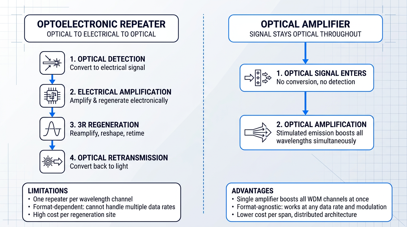
The original answer to signal attenuation was the optoelectronic repeater, a device that detects the incoming optical signal, converts it to an electrical signal, amplifies and regenerates it electronically, then re-converts it back to light and retransmits it down the next fibre span.
This process is known as 3R regeneration: re-amplify, reshape, and retime. The Wikipedia article on optical communications repeaters defines these three functions precisely — reamplification restores signal power, reshaping corrects pulse distortion, and retiming realigns the pulse stream to the clock. 3R regeneration works, and it was the dominant approach in early fibre-optic systems.
As data rates climbed and wavelength-division multiplexing (WDM) emerged — carrying dozens of independent channels at different wavelengths down a single fibre — the limitations of repeaters became acute. The Wikipedia fibre-optic communication article and the IEEE TechNav optical communications repeater resource identify the core problems clearly.
- Cost per span: Each repeater requires optical receivers, electronic amplifiers, and laser transmitters — expensive hardware that must be installed at every regeneration site.
- WDM incompatibility: One repeater handles one wavelength channel. A WDM system with many channels requires a separate repeater chain for each — multiplying cost and complexity enormously.
- Bandwidth rigidity: Each repeater is engineered for a specific data rate and modulation format. Upgrading the system means replacing every repeater along the entire link.
- Format dependence: Because the signal is decoded and re-encoded electrically, repeaters are opaque to the optical signal's bit rate and modulation format — they cannot be format-agnostic.
Repeaters were the engineering solution of their era, and they worked. But the combination of high per-span cost and fundamental incompatibility with multi-channel WDM systems made a different approach necessary as the capacity demands of modern networks grew.
Direct Amplification in the Optical Domain
An optical fibre amplifier takes a fundamentally different approach: it amplifies the optical signal directly, without ever converting it to an electrical signal. As the Wikipedia article on optical amplifiers states, such a device "amplifies an optical signal directly, without the need to first convert it to an electrical signal."
A useful conceptual framing, also drawn from the same Wikipedia source, is that an optical amplifier may be thought of as a laser without an optical cavity — or one in which feedback from the cavity is suppressed. In a conventional laser, a gain medium sits inside a resonant cavity formed by mirrors; the cavity sustains oscillation. Remove the cavity, and the gain medium simply amplifies whatever light passes through it.
The underlying physics, common to most optical amplifiers, is stimulated emission: a gain medium is pumped by an external energy source to create a population inversion, where more atoms or carriers occupy an excited state than the ground state. When an incoming signal photon passes through this inverted medium, it stimulates the emission of an additional photon at the same wavelength, phase, and direction — producing coherent gain.
For Raman amplifiers, the gain mechanism is distinct but conceptually analogous: stimulated Raman scattering (SRS) transfers energy from high-power pump photons to signal photons via the vibrational modes of the glass lattice itself, as noted in the IEEE TechNav optical amplifiers resource. Different amplifier families exploit different physical mechanisms within this shared framework of optical gain — the detailed physics of each belongs to the sections that follow.
Why Optical Amplifiers Displaced Repeaters
The decisive advantage of optical amplification in WDM systems is that a single amplifier boosts all co-propagating wavelength channels simultaneously, without demultiplexing them. The IEEE TechNav WDM networks resource describes this directly: the EDFA "amplifies all wavelength channels simultaneously over the 1530 to 1570 nm band without converting the signal to the electrical domain," replacing what would otherwise be a separate repeater chain for every channel.
Equally important is data-rate transparency. Because an optical amplifier never decodes the signal, it operates independently of bit rate and modulation format. The Wikipedia fibre-optic communication article notes explicitly that optical amplifiers "operate independently of the data rate and modulation format, enabling multiple data rates and modulation formats to coexist and enabling upgrading of the data rate of a system without having to replace all of the repeaters."
Before optical amplifiers, each WDM wavelength channel required its own dedicated repeater chain. A single optical amplifier replaces all of them — simultaneously boosting every channel without demultiplexing, regardless of the data rate or modulation format each channel carries.
The real-world impact was rapid and transformative. According to the IEEE Canadian Review article and a Springer textbook chapter on optical communications, the first transatlantic cable system to use optical amplifiers in place of electronic regenerators was TAT-12/13, which went into service in 1995 — operating at 5.3 Gbit/s with amplifier spacing of approximately 50 km across spans exceeding 5,900 km. The EDFA had moved from laboratory demonstration to intercontinental deployment in under a decade.
The Three Principal Amplifier Families
Three families of optical fibre amplifier dominate both research and commercial deployment, each exploiting a different physical mechanism and suited to different system contexts.
- EDFA (Erbium-Doped Fibre Amplifier): A length of silica fibre doped with erbium ions that exploits stimulated emission from the erbium energy level structure. The dominant technology for long-haul WDM systems.
- Raman Amplifier: Exploits stimulated Raman scattering in the transmission fibre itself. Provides distributed gain along the span and offers wavelength flexibility beyond the EDFA gain band.
- SOA (Semiconductor Optical Amplifier): Uses stimulated emission in a forward-biased semiconductor p-n junction. Compact and electrically pumped; well suited to photonic integrated circuits and datacentre applications.
Each family has a distinct gain mechanism, operating wavelength range, noise characteristics, and application profile. The sections that follow examine them in depth — beginning with the EDFA, which remains the workhorse of long-haul optical communications worldwide.
Erbium-Doped Fibre Amplifiers: Physics and Operation
Of the three principal optical amplifier families, the erbium-doped fibre amplifier (EDFA) is the one that reshaped telecommunications. Introduced commercially in the early 1990s, it did something no previous technology could do cleanly: amplify dozens of wavelength channels simultaneously, in the optical domain, without any electrical conversion, across the precise spectral window where silica fibre loses least light. Understanding why it can do all of this requires going one level deeper than the usual specification catalogue — into the atomic physics of the erbium ion itself.
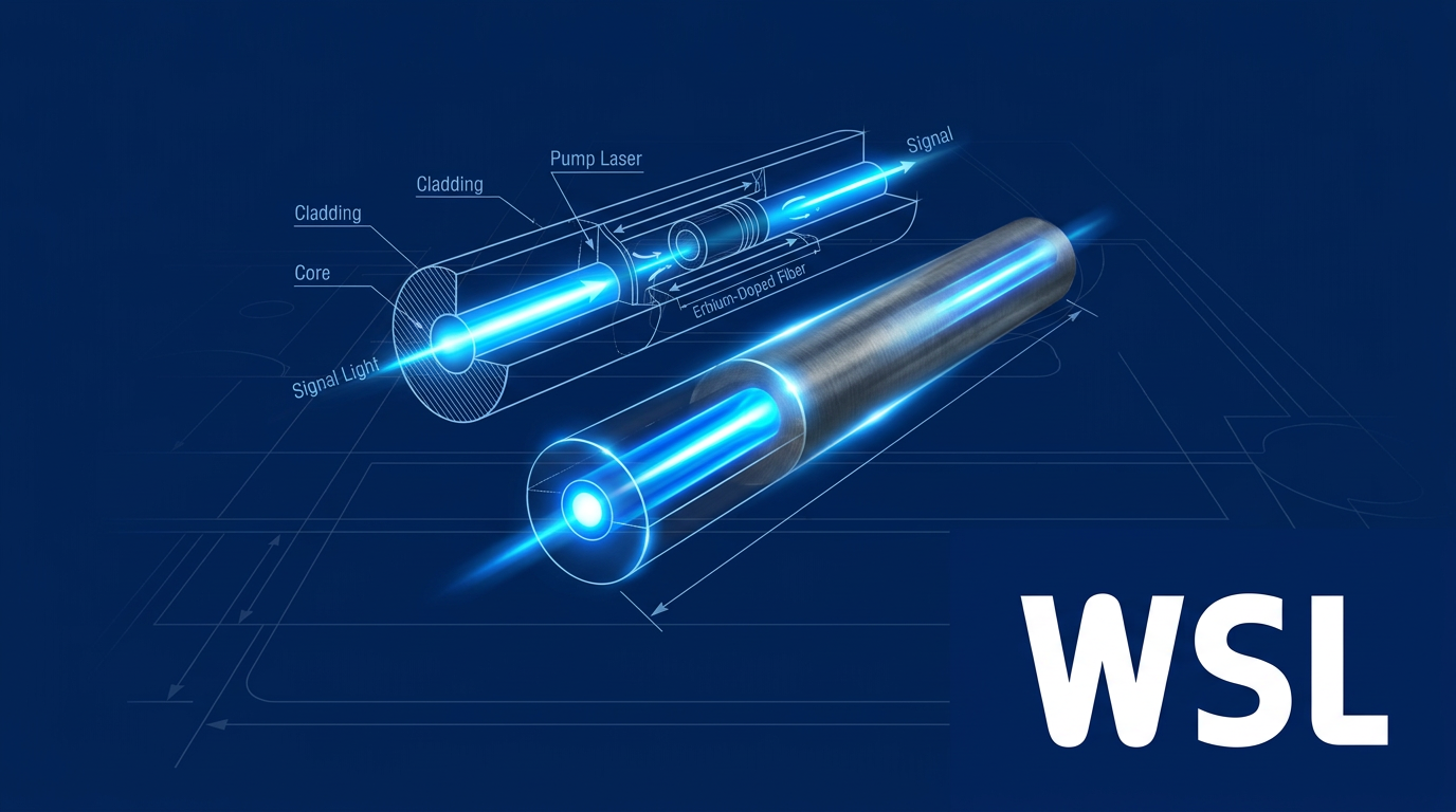
Physically, an EDFA is a compact assembly of three components: a length of silica fibre whose core is doped with trivalent erbium ions (Er³⁺), a pump laser diode, and a WDM coupler that combines the pump and signal wavelengths before they enter the doped fibre.
The doped fibre length is typically around 8–20 metres for short amplifiers, though this must be optimised carefully: too short and the pump photons are not fully absorbed, leaving insufficient gain; too long and the far end of the fibre — where pump power is depleted — contributes noise through amplified spontaneous emission (ASE) rather than useful gain.
The Three-Level Energy System of Er³⁺
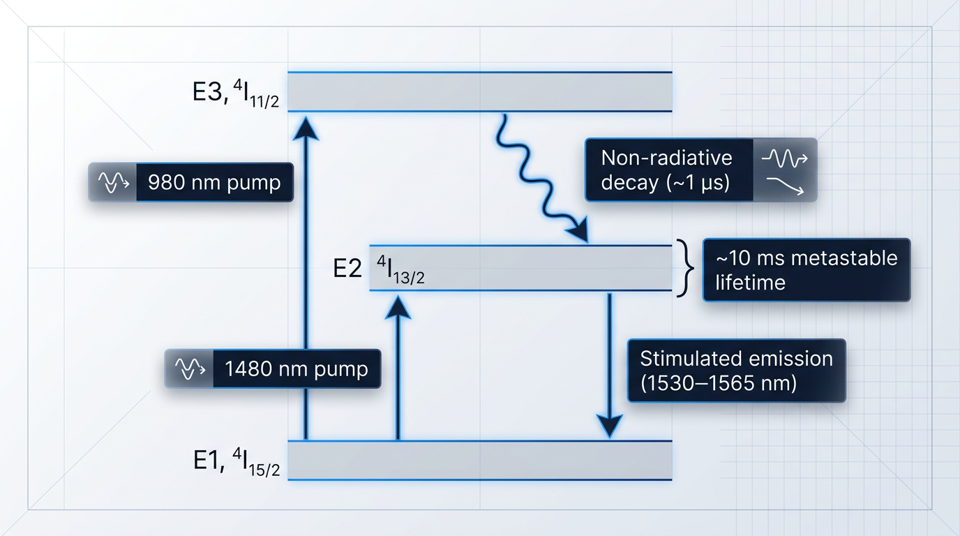
The gain mechanism of an EDFA originates in the quantum energy structure of the Er³⁺ ion embedded in a silica glass host. Three levels are central to the operation: the ground state E1 (spectroscopic notation ⁴I₁₅/₂), the metastable excited state E2 (⁴I₁₃/₂), and the upper pump level E3 (⁴I₁₁/₂).
The decisive physical property of this system is the metastable lifetime of the E2 level, approximately 10 ms — four orders of magnitude longer than the ~1 µs lifetime of the E3 level above it.
This long lifetime is not incidental: it is the physical prerequisite for population inversion. Because ions arriving at E2 linger there for ~10 ms before spontaneously decaying, they accumulate — the E2 population grows large relative to E1, creating the inverted distribution that enables stimulated emission to dominate over absorption.
980 nm vs 1480 nm Pumping: A Design Choice
Two pump wavelengths are used in practice, and the choice between them is not arbitrary — each exploits a different excitation pathway with distinct consequences for amplifier performance.
- 980 nm pumping: Excites E1→E3; ions decay rapidly (~1 µs) to E2. Near-complete population inversion achieved. Lowest noise figure (<4 dB). Preferred for noise-sensitive applications.
- 1480 nm pumping: Excites E1→top of E2 directly. Inversion is incomplete; some ions remain in E1. Higher quantum efficiency (~50%). Preferred for high-output-power applications.
The physics behind this trade-off is precise. At 980 nm, pump photons excite ions all the way to E3, from which they cascade non-radiatively to E2 in ~1 µs. Because the E3 lifetime is too short for stimulated emission to occur there, virtually all ions accumulate in E2 — producing the closest approximation to complete population inversion achievable in a three-level system, and consequently the lowest achievable noise figure.
At 1480 nm, pump photons carry ions directly into the top of the E2 metastable band, bypassing E3 entirely. No energy is lost to the non-radiative E3→E2 transition, which is why the optical conversion efficiency is higher (~50% vs ~35% for 980 nm pumping). However, because the pump and signal share the same energy manifold, some ions remain in E1 — inversion is incomplete, and the minimum achievable noise figure rises to around 5.5 dB.
The practical implication is that the pump wavelength is a design lever, not a fixed parameter: 980 nm is the choice where noise figure is the critical constraint, while 1480 nm is favoured where maximum output power is the priority. The physical reasons for this distinction will directly inform the amplifier configuration choices discussed later in this guide.
| Parameter | 980 nm pump | 1480 nm pump |
|---|---|---|
| Excitation pathway | E1 → E3, then non-radiative decay to E2 | E1 → top of E2 directly |
| Population inversion | Near-complete | Incomplete (some ions remain in E1) |
| Minimum noise figure | <4 dB | ~5.5 dB |
| Optical conversion efficiency | ~35% | ~50% |
| Module wall-plug efficiency | ~39% W/W | ~13% W/W |
| Preferred application | Low-noise, noise-sensitive stages | High-output-power stages |
Quantitative comparison of 980 nm and 1480 nm pump sources across key performance parameters, grounded in UCSB ECE228 lecture data, making the noise figure vs efficiency trade-off explicit.
The table makes the trade-off concrete: 980 nm pumping delivers a superior noise figure and higher wall-plug efficiency, while 1480 nm pumping converts a greater fraction of pump photons into signal photons at the optical level — making it the logical choice when output power is the binding constraint rather than noise.
Stimulated Emission and the Gain Mechanism
With the Er³⁺ ions accumulated in E2, the gain mechanism operates as follows: an incoming signal photon in the 1530–1565 nm wavelength range interacts with an excited ion and stimulates it to emit a second photon at exactly the same wavelength, phase, and propagation direction as the original. This is stimulated emission — the process that produces coherent optical gain.
The reason the gain band sits where it does — centred near 1550 nm rather than at some other wavelength — comes directly from the energy gap between E2 and E1 in the erbium ion. But the reason that gain band is broad rather than a narrow atomic line is a consequence of the amorphous silica glass host.
In a crystalline host, each Er³⁺ ion sits in an identical local environment, and transitions occur at a sharp, well-defined frequency. In amorphous glass, each ion experiences a slightly different local electric field, shifting its transition frequency by a different amount through the Stark effect. The ensemble of ions therefore spans a continuous distribution of transition frequencies — a process called inhomogeneous broadening — with thermal redistribution among the Stark-split sublevels (thermalisation) adding further spectral smearing.
The result is a gain spectrum spanning tens of nanometres rather than a few picometres, and it is this broadening that makes a single EDFA capable of amplifying many WDM channels simultaneously — each on a different wavelength within the band.
Gain Bands: C-Band, L-Band, and Key Parameters
The primary EDFA gain window is the C-band, spanning approximately 1530–1565 nm, with a gain peak near 1530 nm and a relatively flat region extending toward 1560 nm. The L-band (1565–1625 nm) is accessible by operating the amplifier at lower inversion levels — typically 35–40% mean inversion — using longer doped fibre lengths, at the cost of reduced efficiency.
The fact that these bands coincide with silica fibre's lowest-attenuation window is not a coincidence: it is precisely why erbium was selected as the dopant. The ⁴I₁₃/₂ → ⁴I₁₅/₂ transition wavelength of Er³⁺ in glass matches the minimum-loss region of silica fibre, making the technology a natural fit for long-haul communications.
Typical small-signal gain for a well-designed EDFA ranges from 20 to 40 dB. The noise figure has a quantum-limited theoretical minimum of 3 dB, with practical devices achieving 4–6 dB depending on pump power, fibre length, and inversion level.
The amorphous structure of the silica host creates a continuous distribution of Er³⁺ transition frequencies through Stark splitting and thermalisation. This inhomogeneous broadening transforms a narrow atomic line into a gain band wide enough to amplify dozens of WDM channels simultaneously — without it, EDFA would be a narrowband device unsuitable for modern fibre networks.
Why EDFA Dominates Long-Haul WDM
The system-level advantages of EDFA are not a separate topic from its physics — they follow directly from the properties already established above.
Data-rate transparency arises because the gain mechanism is purely optical: the EDFA amplifies photons regardless of how they are modulated, with no knowledge of bit rate or modulation format.
Low inter-channel crosstalk is a direct consequence of the ~10 ms metastable lifetime at E2. Because the gain dynamics respond on a millisecond timescale, the amplifier cannot follow the nanosecond-scale fluctuations of individual data bits — it responds only to average total power, so rapid power variations in one channel do not corrupt adjacent channels.
Polarisation insensitivity follows from the amorphous glass host: the random orientation of Er³⁺ ions throughout the fibre means the ensemble gain is independent of the polarisation state of the input signal, removing a significant engineering burden from system designers.
High pump-to-signal conversion efficiency — particularly at 980 nm where wall-plug efficiency reaches ~39% — combined with the ability to amplify all WDM channels through a single device, makes EDFA the most cost-effective amplification technology for dense wavelength-division multiplexed systems at scale.
With EDFA's physics established — from the atomic energy levels through to the system-level advantages they produce — the next section turns to Raman fibre amplifiers, which exploit an entirely different physical process and offer a complementary set of performance characteristics.
Explore Custom EDFAs Built for Your Application
EDFA technology is highly application-specific. View the company's tailored EDFA solutions, or download a datasheet to review specifications for your system requirements.

Raman Fibre Amplifiers: Distributed Gain and Wavelength Flexibility
Unlike EDFA, which requires a specially prepared length of erbium-doped fibre as its gain medium, the Raman fibre amplifier uses something already present in every optical link: the transmission fibre itself.
The mechanism responsible is stimulated Raman scattering (SRS) — an inelastic interaction between a pump photon and the silica glass lattice that requires no dopant, no population inversion, and no specially fabricated gain element.
The Stimulated Raman Scattering Mechanism
When a high-power pump photon propagates through silica fibre, it interacts with the vibrational modes of the glass network — the optical phonons of the lattice — through inelastic scattering.
In this interaction, the pump photon transfers a portion of its energy to the lattice as molecular vibration, and the remaining energy emerges as a new, lower-frequency photon that coherently amplifies the co-propagating signal.
The gain arises purely from the scattering physics of the host glass — not from population inversion in a dopant ion, as with erbium in an EDFA — which means any silica fibre is, in principle, a potential gain medium.
Pump-Signal Wavelength Relationship and Spectral Flexibility
Raman gain in silica peaks at a characteristic frequency offset below the pump frequency, with the pump-signal wavelength separation falling in the region of approximately 100 nm at wavelengths near 1550 nm.
The practical implication is direct: the pump wavelength is the engineer's primary design handle for positioning the gain band anywhere in the spectrum.
Unlike EDFA, whose gain band is fixed by erbium's spectroscopy to the C-band and extendable to the L-band, Raman amplification is viable in the S-band (approximately 1460–1530 nm) and other spectral regions where EDFA cannot operate.
Multi-pump configurations extend this further: by launching several pump wavelengths simultaneously, the composite Raman gain spectrum can be shaped to cover S-, C-, and L-bands together, producing a broad gain profile attractive for wideband WDM systems.
Distributed vs. Lumped Raman Amplification
The most architecturally significant distinction in Raman amplifier design is between distributed Raman amplification (DRA) and lumped Raman amplification.
In a lumped configuration, a discrete length of Raman-gain fibre is inserted at a specific point in the link — functionally analogous to an EDFA node, though without doping.
In distributed amplification, pump light is launched counter-propagating into the far end of a transmission span, so the span fibre itself provides continuous gain along its length rather than at a single node.
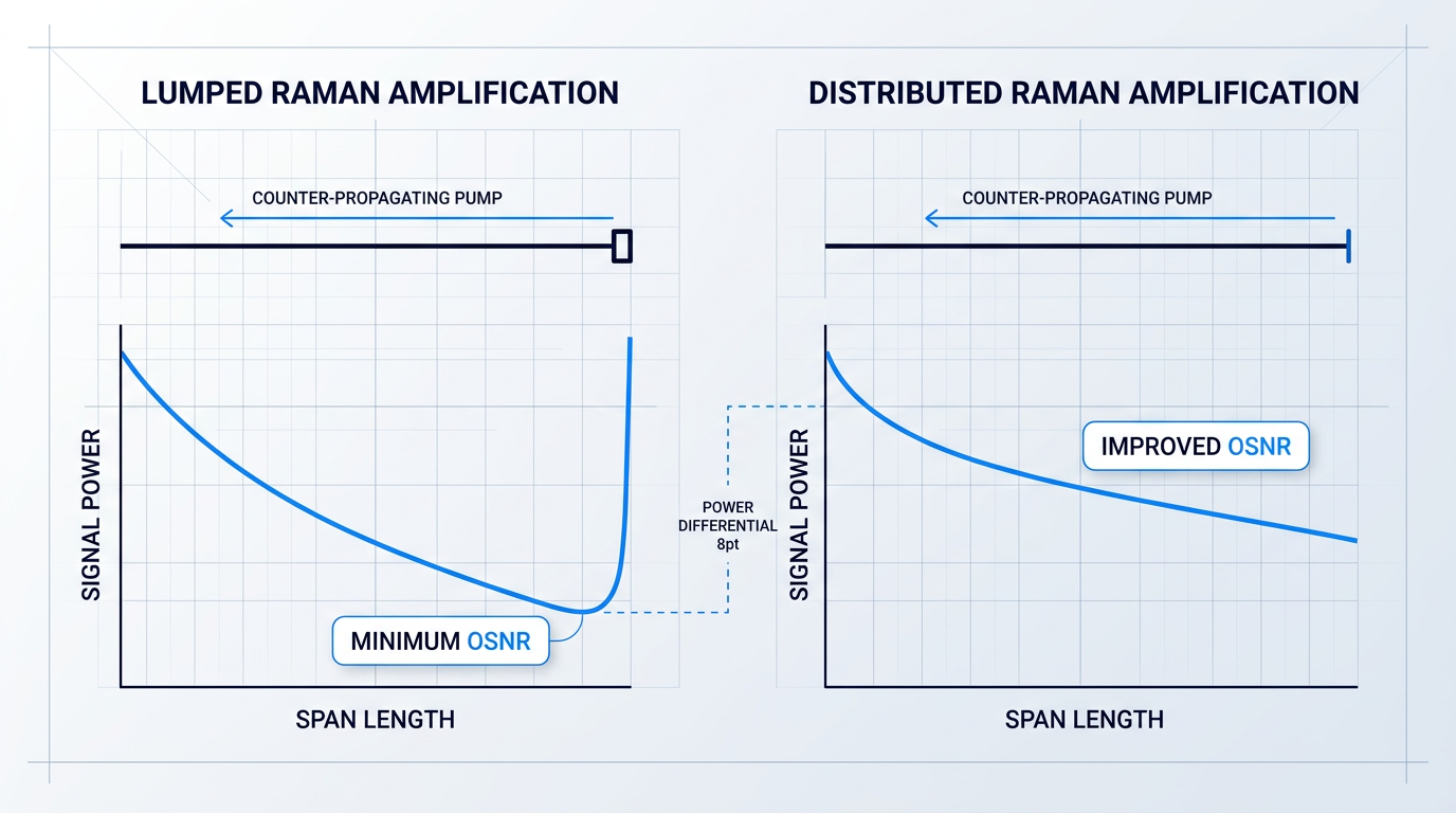
The OSNR advantage of DRA follows directly from this architecture: in a purely lumped system, the signal decays over the full span length before being amplified at the node, reaching its lowest power — and worst signal-to-noise ratio — just before the amplifier.
With distributed Raman gain applied continuously along the span, the signal never decays as far, because gain is delivered progressively before the signal power has collapsed.
This improved signal power floor throughout the span translates into a meaningful OSNR advantage over purely lumped architectures — a benefit that becomes increasingly significant as span lengths and channel counts grow.
Because distributed Raman gain is applied continuously along the span rather than at the end of it, the signal power floor is higher throughout the link — the signal never decays as far before gain is applied. This is a structural OSNR advantage that no lumped amplifier configuration can replicate.
In practice, DRA is most commonly deployed as a pre-amplification stage within a hybrid Raman/EDFA configuration: distributed Raman gain improves OSNR over each span, and a lumped EDFA at the amplifier node provides the bulk power restoration.
This hybrid architecture is the standard approach in ultra-long-haul terrestrial links and submarine cable systems, where OSNR margins are the critical constraint.
Engineering Constraints: Pump Power and Polarisation
Raman amplification's system advantages come with real engineering costs, two of which dominate practical deployment decisions.
- High pump power demand: The Raman gain coefficient in standard silica fibre is small, requiring substantially higher pump powers than EDFA — driving up component cost and introducing safety considerations at the fibre launch point.
- Dispersion-compensating fibre efficiency: DCF has a much smaller core than standard single-mode fibre, producing higher optical intensity for a given pump power and making it a more efficient Raman gain medium for lumped configurations.
- Polarisation-dependent gain: Raman gain is strongly polarisation-sensitive — copolarised pump-signal gain is significantly higher than orthogonally polarised gain, causing effective gain to fluctuate as signal polarisation varies along the fibre.
- Depolarised pump mitigation: Practical systems suppress polarisation-dependent gain by combining two pump diodes with orthogonal polarisation states before launch, presenting an averaged, stable gain to the signal regardless of its polarisation state.
The pump power requirement is not merely a cost consideration: at the levels needed for meaningful Raman gain in standard fibre, safety protocols for the fibre launch point become a genuine operational concern, particularly in field-deployed systems.
Polarisation-dependent gain (PDG) is the subtler constraint — because signal polarisation rotates continuously along the fibre due to birefringence, an unmitigated polarised pump would produce gain that fluctuates with that rotation, adding a noise-like component that degrades system performance.
The depolarised pump approach is now standard practice: by combining two pump diodes with orthogonal polarisation states before launch, the pump presents both polarisation axes simultaneously, and the gain averages to a stable, polarisation-insensitive value.
With these constraints understood, the Raman amplifier's position in the amplifier landscape becomes clear: it is the technology of choice when OSNR performance or wavelength coverage requirements exceed what EDFA alone can deliver, accepted in exchange for greater system complexity and pump power investment.
The third principal optical fibre amplifier family — the semiconductor optical amplifier — operates on a different physical mechanism again, and occupies a distinct application niche that the next section addresses.
Semiconductor Optical Amplifiers: Structure, Gain, and Use Cases
The semiconductor optical amplifier (SOA) shares its fundamental gain mechanism with the EDFA — stimulated emission — but in almost every other respect it is a different class of device entirely. Where an EDFA is a metre-scale length of doped glass fibre pumped by an infrared laser, an SOA is a millimetre-scale semiconductor chip driven by electrical current injection, fabricated using the same compound semiconductor processes as a laser diode and small enough to integrate onto a photonic chip.
That distinction in form factor and pumping approach is not incidental: it is precisely what makes SOAs the right tool in contexts where EDFA cannot go.
Device Structure: The Travelling-Wave Amplifier
Structurally, an SOA is nearly identical to a Fabry-Perot laser diode: a forward-biased semiconductor p-n junction with an active waveguide region through which light propagates.
The critical difference is what happens at the facets. In a laser diode, cleaved facets act as partial mirrors, providing the optical feedback that sustains lasing. In an SOA, both facets receive anti-reflection (AR) coatings — typically achieved by combining a dielectric AR layer with angled facets — reducing residual reflectivity to below 10⁻⁴.
Suppressing that feedback prevents self-oscillation, converting the device from an oscillator into a single-pass travelling-wave amplifier: light enters one facet, is amplified across the active region (typically 500–600 µm of active section), and exits the other facet without bouncing back.
Achieving residual reflectivity below 10⁻⁴ is what separates a true travelling-wave SOA from a resonant SOA: at that threshold, gain ripple falls below 0.5 dB and the optical bandwidth exceeds 5 THz — sufficient to cover the full C-band and beyond.
Gain Mechanism: Current Injection and Stimulated Recombination
Injecting current into the p-n junction elevates electrons into the conduction band and leaves holes in the valence band, establishing population inversion in the active region — the semiconductor analogue of the population inversion encountered in the EDFA's erbium ions.
When a signal photon enters the active waveguide, it triggers stimulated electron-hole recombination: an electron drops from the conduction band to fill a hole in the valence band, releasing a second photon at the same wavelength and phase as the incoming one.
The gain condition requires that the quasi-Fermi level separation exceed the photon energy — the semiconductor equivalent of population inversion — and is sustained by continuous current injection rather than by an optical pump laser, as in EDFA.
Wavelength Coverage and Active Layer Design
One of the SOA's genuine structural advantages over EDFA is wavelength flexibility. The EDFA's gain band is fixed by the spectroscopy of erbium ions in silica glass. The SOA's gain band, by contrast, is set by the bandgap of the semiconductor material in the active layer — a parameter the designer controls through material composition.
By selecting the appropriate compound semiconductor alloy (InGaAsP, InGaAs, GaInNAs, and others on InP or GaAs substrates), an SOA can be engineered to operate across the O-band (~1260–1360 nm), S-band, C-band, or L-band — as confirmed by commercial devices spanning 1050 nm to 1625 nm.
Quantum-well active regions extend the gain bandwidth further: by confining carriers in a thin well layer, quantum confinement produces a density-of-states structure that broadens the gain spectrum, with 3 dB bandwidths reaching 80–105 nm in commercial C-band devices.
Strained quantum wells — where the well material is deposited with a slight lattice mismatch relative to the substrate — address a separate problem: the biaxial strain splits the heavy-hole and light-hole valence bands, partially equalising the gain for TE and TM polarisations and reducing the polarisation-dependent gain (PDG) that would otherwise make the device sensitive to signal polarisation state.
Gain Dynamics: SOA's Central Trade-Off
The most consequential difference between SOA and EDFA performance in WDM systems is the speed of the gain response. The carrier lifetime in a semiconductor active region is on the order of 1 ns — confirmed by experimental measurements attributing this to nonradiative recombination at heterojunction interfaces — orders of magnitude shorter than the millisecond-scale upper-state lifetime of erbium ions established in the EDFA section of this guide.
Because EDFA's gain recovers on a millisecond timescale, bit-level power fluctuations at gigabit-per-second data rates are far too fast to perturb the erbium population inversion: the gain is effectively constant across all channels, making EDFA naturally immune to inter-channel crosstalk in WDM.
An SOA's nanosecond carrier lifetime means its gain does respond to bit-level power changes. In a multichannel WDM system, power fluctuations in one channel can saturate or partially deplete the gain medium, modulating the gain seen by every other channel simultaneously — a phenomenon called cross-gain modulation (XGM).
Within a single channel, the same fast response produces pattern-dependent distortion: the gain available to a given bit depends on the power history of recent preceding bits, causing the signal eye to close at high data rates when the SOA is operating in saturation.
The practical consequence for multichannel linear amplification is clear: SOAs must be operated in the unsaturated gain regime, where input powers are low enough that the gain medium is not significantly depleted by any single channel — a real constraint on launch power and system design.
The nanosecond carrier lifetime that causes XGM crosstalk in linear WDM amplification is the identical physics that enables wavelength conversion in nonlinear operation. Whether fast gain dynamics are a problem or a capability depends entirely on the operating regime — saturated or unsaturated.
When an SOA is deliberately driven into saturation, XGM becomes a tool: a data-modulated pump signal at one wavelength depletes the carrier population, imprinting its modulation pattern onto a continuous-wave probe at a different wavelength as an inverted amplitude copy. Cross-phase modulation (XPM) offers a related mechanism — the carrier density change modulates the refractive index of the active waveguide, producing a phase shift on the probe that a Mach-Zehnder interferometer can convert to amplitude modulation with non-inverted output.
These effects enable all-optical wavelength conversion, signal regeneration, and clock recovery — functions that exploit SOA nonlinearity deliberately rather than treating it as a defect.
Noise Figure and Polarisation-Dependent Gain
SOAs exhibit noise figures ranging from 8 dB to 11.5 dB in practical packaged devices — higher than EDFA — and two distinct physical mechanisms contribute.
The first is amplified spontaneous emission (ASE) generated within the active region, which is present in any optical amplifier. The second is specific to the SOA's chip-in-fibre architecture: light must be coupled from optical fibre into the semiconductor waveguide at the input, and back out into fibre at the output, incurring coupling losses of 1.5–2.5 dB per interface. Because input coupling loss appears before the gain stage, a 1 dB increase in input coupling loss raises the noise figure by 1 dB directly.
Residual polarisation-dependent gain is a further system consideration. Even with strained quantum-well active layers, practical SOA devices exhibit PDG of approximately 1.0 dB typical, up to 2.5 dB maximum — meaning a signal's TE and TM components are amplified by slightly different amounts. In networks where signal polarisation is not actively controlled, this PDG introduces amplitude uncertainty that must be budgeted in system margin.
These are genuine engineering trade-offs, not disqualifying flaws. The noise figure penalty is the price of electrical pumping and chip-scale integration — a price that is entirely acceptable in the application domains where SOAs are the right choice.
The table below places SOA specifications in direct comparison with EDFA on the axes that matter most for system design decisions.
| Parameter | SOA | EDFA |
|---|---|---|
| Noise Figure | 8–11.5 dB (8 dB typ. / 9.5 dB max for SOA1013S; 10 dB typ. / 11.5 dB max for SOA1117S) | 4–6 dB in practical devices (3 dB quantum limit) |
| Gain Dynamics (carrier/upper-state lifetime) | ~1 ns (nonradiative recombination at heterojunction interfaces) | Millisecond-scale (~10 ms; slow relative to bit periods at Gbit/s rates) |
| Typical Small Signal Gain | 13–30 dB depending on device (SOA1013S: 13 dB; BOA C-band: 27–35 dB) | 20–40 dB |
| Gain Bandwidth (3 dB) | 70–105 nm in commercial C-band devices; O/S/L-band devices also available | ~35 nm in the C-band (1530–1565 nm); fixed by Er³⁺ spectroscopy |
| Wavelength Coverage | O, S, C, L bands selectable by semiconductor material composition (1050–1625 nm) | C-band and L-band; fixed by erbium ion spectroscopy in silica |
| Pump Type | Electrical current injection (typically 500–750 mA operating current) | Optical pump laser (980 nm or 1480 nm) |
| Form Factor | Chip: ~1–1.5 mm active length; packaged in butterfly module or benchtop unit | Fibre coil: metres of rare-earth-doped fibre plus pump laser and WDM coupler |
| Polarisation-Dependent Gain | ~1.0 dB typical; up to 2.5 dB max (strained QW partially mitigates) | Negligible — the amorphous glass host makes EDFA gain polarisation-insensitive |
| WDM Multichannel Crosstalk | XGM crosstalk when saturated; unsaturated operation required for linear WDM | Negligible — millisecond gain dynamics cannot follow bit-rate fluctuations |
Side-by-side comparison of SOA and EDFA on key quantitative performance axes. SOA figures are drawn from Thorlabs datasheets and SPIE/IEEE research.
The SOA data in the table is grounded in Thorlabs device specifications across two product families: the SOA1013S (polarisation-insensitive, C-band) and SOA1117S (polarisation-maintaining, C-band), representing the range of practical packaged devices.
The pattern the table makes visible is this: SOA's wider wavelength coverage and chip-scale form factor are genuine, sourced advantages, while its higher noise figure and susceptibility to XGM in saturation are real constraints that define where it belongs in a system architecture. No single amplifier technology dominates on every axis.
Where SOAs Are the Right Choice
In photonic integrated circuits (PICs) and silicon photonics, the SOA's compactness and electrical pumping are not compromises relative to EDFA — they are requirements. Silicon cannot produce efficient optical gain through stimulated emission, and an EDFA's metre-scale fibre coil and optical pump laser have no place on a chip. Heterogeneous integration of III-V SOA gain elements with silicon waveguide circuits is an active commercialisation direction, providing the gain element that PIC architectures cannot otherwise source.
In datacentre interconnects and metro networks, SOAs serve as booster amplifiers in compact transmitter modules, increasing launch power after modulation in short-reach links where the bulk of an EDFA system would be impractical. A single SOA can amplify multiple WDM channels simultaneously, making it efficient in space-constrained transceiver designs.
In optical switching and gating applications — reconfigurable optical add/drop multiplexers (ROADMs), burst-mode systems, and fast optical shutters — the nanosecond switching speed that creates XGM problems in linear amplification becomes a direct asset. SOA-based optical gates with 1 ns switching speeds and extinction ratios exceeding 60 dB are available in commercial devices, enabling rapid channel routing without optical-to-electrical conversion.
For all-optical signal processing — wavelength conversion, 2R regeneration, clock recovery — SOA nonlinearity is the functional mechanism rather than a side effect. XGM-based wavelength converters transfer data between wavelengths at rates up to 40 Gbit/s; XPM-based Mach-Zehnder configurations extend this capability with non-inverted output. These functions make SOAs the gain element of choice in photonic switching nodes and optical processing subsystems.
Understanding how each amplifier type behaves at the device level — its gain mechanism, dynamics, noise characteristics, and wavelength coverage — is the necessary foundation for the next question: how do these devices perform as components within a real transmission system, where noise accumulates across cascaded amplifier stages and gain saturation interacts with WDM channel loading across hundreds of kilometres?
Noise, Gain Saturation, and Bandwidth: System-Level Performance
Understanding how each amplifier type works is necessary but not sufficient for real deployment decisions — what matters equally is how an amplifier behaves when it is one of dozens in a cascaded chain, where its noise, saturation characteristics, and gain spectrum interact cumulatively with every other stage.
Amplified Spontaneous Emission and Noise Figure
Every optical amplifier, regardless of type, generates amplified spontaneous emission (ASE) as an inescapable by-product of population inversion: spontaneously emitted photons that happen to propagate along the fibre waveguide are amplified alongside the signal, producing a broadband noise floor that accumulates with every amplifier in the chain.
Noise figure (NF) is the standard metric for quantifying how much an amplifier degrades the signal-to-noise ratio. The theoretical quantum limit is 3 dB, derived from the minimum spontaneous emission factor of 1 achievable in a fully inverted gain medium; practical EDFAs reach 4–6 dB due to incomplete inversion, insertion loss, and component imperfections, while SOAs carry a higher penalty of 6–10 dB driven by fibre-chip coupling losses and elevated internal loss.
Distributed Raman amplification is the notable outlier: because gain accumulates before the signal power has decayed to its minimum in the span, the effective noise figure referred to the span input can fall below 0 dB — a genuine advantage over lumped-amplifier-only architectures that directly improves OSNR at the end of each span.
Optical signal-to-noise ratio (OSNR), conventionally measured in a 0.1 nm (12.5 GHz) reference bandwidth, is the master design parameter for cascaded amplifier chains. The dominant impairment at the receiver is signal-ASE beating — coherent interference between the signal and co-propagating ASE that produces electrical noise proportional to the product of signal power and ASE spectral density — and OSNR sets the achievable bit error rate and therefore the fundamental reach limit of the link.
In a chain of N identical amplifiers, OSNR degrades approximately as 1/N, which is why amplifier spacing and noise figure minimisation are central to long-haul link budget engineering.
Because OSNR degrades as 1/N across N amplifiers, halving the noise figure of each stage or halving the number of stages both double the achievable OSNR — making low-NF amplifiers and careful span design the two primary levers for extending link reach.
Gain Saturation: Physical Cause and Amplifier-Specific Behaviour
Gain saturation occurs when increasing input signal power causes the amplifier's gain to fall below its small-signal value: stimulated emission depletes the population inversion faster than the pump can replenish it, reducing available gain. The standard figure of merit is saturation output power (P_sat), defined as the output power at which gain has compressed by 3 dB relative to the small-signal value.
- EDFA saturation: Slow ~10 ms gain dynamics suppress WDM inter-channel crosstalk but create sensitivity to channel add/drop transients in reconfigurable networks, requiring dynamic gain control.
- SOA saturation: Nanosecond carrier lifetimes cause pattern-dependent gain distortion and inter-channel crosstalk; WDM applications require operation in the unsaturated regime, limiting output power.
- Raman saturation: Arises from pump depletion rather than inversion depletion; pump power fluctuations translate directly into gain fluctuations, with onset generally less abrupt than EDFA.
These differences carry direct system design consequences: the SOA's fast gain dynamics restrict it to unsaturated operation in any multichannel linear amplification role, while the EDFA's slow response — beneficial for WDM crosstalk suppression — demands active transient control in reconfigurable optical add/drop multiplexer (ROADM) networks where channel loading changes abruptly.
Bandwidth, Gain Flatness, and WDM Compatibility
EDFA gain is not uniform across the C-band: it peaks near 1530 nm and tapers toward the band edges, spanning roughly 35 nm (1530–1565 nm). In a single amplifier this non-uniformity is manageable, but across a cascade of 20–40 amplifiers — as found in transoceanic links — channel power divergence accumulates exponentially, leaving channels near the gain peak orders of magnitude stronger than those at the band edges.
The standard engineering solution is the gain-flattening filter (GFF), inserted at the mid-stage access point of a dual-stage EDFA design, between the first and second gain stages. The GFF applies a spectrally shaped attenuation that is the inverse of the EDFA gain spectrum, equalising channel powers without degrading noise figure (the first stage has already provided gain before the filter) or output power (the second stage restores it afterwards).
| Amplifier Type | Wavelength Band | Approximate Bandwidth (nm) | Gain Flatness / WDM Notes |
|---|---|---|---|
| EDFA (C-band) | 1530–1565 nm | ~35 nm | Non-uniform gain; GFF required for dense WDM cascades beyond a few spans. |
| EDFA (L-band) | 1565–1625 nm | ~60 nm | Extends total EDFA coverage; typically paired with C-band EDFA for wideband WDM. |
| Multi-pump Raman (S+C+L) | 1460–1625 nm | ~165 nm (combined) | Broadest coverage; gain flatness set by pump wavelength and power optimisation. |
| SOA | Varies by material; typically 1250–1650 nm range | 40–100 nm | Wide raw bandwidth; gain flatness requires careful bias control; PDG a concern. |
Comparison of optical amplifier types by wavelength band coverage and approximate bandwidth, to support WDM system design decisions.
The table makes a key trade-off explicit: EDFA offers the most mature and spectrally flat solution within its bands when GFFs are applied, but its coverage is fixed by the erbium ion's emission spectrum. Multi-pump Raman amplification provides the widest aggregate bandwidth across S+C+L bands, making it the technology of choice when channel plans must extend beyond the C-band without deploying separate amplifier types for each band.
Bandwidth and gain flatness are not secondary specifications — for a dense WDM system engineer, they determine whether a given amplifier technology is viable for a particular channel plan at all. With noise figure, gain saturation, and bandwidth now established as the three governing performance parameters, the natural next question is how each one determines the role an amplifier plays within the system architecture — the subject of the next section on booster, in-line, and pre-amplifier configurations.
Amplifier Configurations: Booster, In-Line, and Pre-Amplifier
Knowing how an EDFA works is necessary — but it is not sufficient for system design. The same erbium-doped fibre amplifier technology, specified differently, performs three structurally distinct jobs in a transmission link: launching maximum power from the transmitter, periodically restoring signal levels across intermediate spans, and conditioning a weak signal before the receiver. Each position presents a different signal power environment, a different OSNR context, and a different set of consequences if the wrong parameter is optimised. The role an amplifier plays determines which specification matters most — and getting that mapping wrong is one of the more consequential mistakes in link engineering.
The three configurations — booster (power) amplifier, in-line amplifier, and pre-amplifier — are not merely labels for the same device placed at different points. They represent different optimisation targets, different pump wavelength choices, and in the case of the in-line role, an architectural tension that requires a two-stage solution to resolve.
Booster Amplifier
The booster sits immediately after the transmitter, and its job is straightforward: launch the highest possible optical power into the first fibre span. Because the input signal arrives directly from the transmitter, the signal-to-noise ratio at the booster's input is already good — the signal has not yet traversed any lossy fibre. This means noise figure is not the critical specification for a booster; the dominant parameters are saturation output power, power conversion efficiency, and the ability to handle high input powers without excessive gain compression.
In practice, booster amplifiers are operated into or near saturation, targeting output powers of +20 dBm or higher. Gain flatness across WDM channels is a secondary concern at this stage — total launched power matters more than spectral uniformity, which can be managed further along the link. For pump choice, 1480 nm pumping (or bidirectional pumping) is preferred at the booster stage because it achieves higher optical-to-signal power conversion efficiency (~50%) compared with 980 nm pumping (~35%), as documented in UCSB ECE228B lecture data. Where compactness and electrical pumping outweigh the noise advantage of EDFA — in datacentre interconnects and metro transmitter applications — SOAs are used in the booster role, taking advantage of their small form factor and on-chip integrability.
In-Line Amplifier
In-line amplifiers are placed at intermediate points along the link — typically every 80–100 km in long-haul terrestrial systems — to compensate for the accumulated span attenuation of roughly 20–30 dB per span. This is the most demanding configuration, because it must simultaneously satisfy two partially competing objectives: high output power to drive the next span, and low noise figure to avoid degrading the OSNR across the cascaded chain.
Both requirements are non-negotiable. Output power sets the launch level into the next span; noise figure determines how much ASE each amplifier contributes, and in a chain of N amplifiers the OSNR degradation is cumulative — each stage's noise figure adds directly to the aggregate noise floor. Gain flatness is particularly critical in the in-line role for WDM systems: as established in §7, spectral non-uniformity compounds across cascaded stages, and even a 1 dB per-amplifier gain tilt can produce a 10 dB channel power divergence after ten stages, rendering the weakest channels undetectable. The in-line amplifier is where the competing requirements are hardest to reconcile — which is precisely what motivates the two-stage architecture discussed below.
Pre-Amplifier
The pre-amplifier sits immediately before the receiver, where the signal has been attenuated across the final span and arrives at its lowest power level in the entire link. The receiver's sensitivity and achievable bit error rate are directly determined by the OSNR of the signal entering it, which makes the pre-amplifier's noise figure the dominant specification. At low input signal powers, ASE generated by the amplifier itself competes directly with the signal; a high noise figure at this stage degrades BER in a way that no downstream processing can correct. The target noise figure for a pre-amplifier is typically below 4 dB, consistent with the minimum achievable in practice for 980 nm-pumped EDFAs.
Output power is not the priority here — the receiver requires only enough signal to detect reliably, not enough to drive a long span. 980 nm pumping is strongly preferred for pre-amplifiers because it achieves complete population inversion at the input end of the gain fibre, minimising the spontaneous emission factor and delivering the lowest achievable noise figure. In short-reach links — particularly metro and access applications — SOAs are used as pre-amplifiers where compactness is valued and the higher noise figure (typically 6–10 dB for SOAs versus sub-4 dB for a well-designed EDFA pre-amplifier) is an acceptable trade-off given the shorter accumulated noise budget.
The table below consolidates the three configurations across the key specification axes, using figures drawn from UCSB ECE228B lecture data and RP Photonics reference material.
| Configuration | Position in Link | Primary Optimisation Target | Noise Figure Target | Output Power Target | Preferred Pump Wavelength(s) |
|---|---|---|---|---|---|
| Booster (Power) Amplifier | Immediately after transmitter | Saturation output power and power conversion efficiency | Secondary — not critical (input SNR already high) | ≥+20 dBm | 1480 nm or bidirectional (higher conversion efficiency ~50%) |
| In-Line Amplifier | Every 80–100 km along long-haul link | Balance of high output power AND low noise figure simultaneously | Moderate — typically 4–6 dB (cumulative OSNR impact) | High — must drive next full span | Bidirectional or 980 nm first stage + 1480 nm second stage (two-stage design) |
| Pre-Amplifier | Immediately before receiver | Minimum noise figure to maximise receiver sensitivity | <4 dB — dominant specification | Low — sufficient for detection only | 980 nm (complete population inversion, lowest noise figure <4 dB) |
Comparison of the three EDFA amplifier configurations across position in link, primary optimisation target, noise figure target, output power target, and preferred pump wavelength, using published reference figures.
The table makes the trade-off structure explicit. Noise figure and output power are inversely prioritised across the three roles: the booster maximises output power and treats noise figure as secondary; the pre-amplifier does the opposite; and the in-line amplifier sits at the uncomfortable intersection of both, unable to sacrifice either. This is not a limitation of any particular product — it is a fundamental consequence of the physics of quasi-three-level gain media, where achieving the highest population inversion for low noise figure and achieving the highest pump-to-signal conversion efficiency for output power pull in different directions.
For an engineer specifying amplifiers for a new link, the table provides the decision framework: identify the position, identify the dominant specification, and select pump wavelength and doped fibre length accordingly. The in-line case, however, demands a more sophisticated answer — which is why the two-stage EDFA architecture exists.
Multi-Stage EDFA Design and Mid-Stage Access
A single-stage EDFA cannot simultaneously optimise noise figure and output power at the level demanded by long-haul DWDM in-line amplification. Achieving the lowest noise figure requires high population inversion at the signal input end of the gain fibre — which points to 980 nm forward pumping and a short, highly inverted doped fibre. Achieving high output power requires high pump power and sufficient doped fibre length to convert that pump energy efficiently — which points to 1480 nm or bidirectional pumping and a longer gain fibre operating at a lower average inversion. These two sets of conditions are incompatible within a single stage.
The engineering solution is the two-stage EDFA: a first stage optimised for low noise figure (high inversion, 980 nm forward pumping, short erbium-doped fibre) followed by a second stage optimised for high output power (1480 nm or bidirectional pumping, longer doped fibre at lower inversion). As documented in UCSB ECE228B lecture materials and RP Photonics tutorial references, this architecture is standard for in-line amplifiers in DWDM long-haul systems precisely because it decouples the two optimisation problems into separate stages.
The critical enabling feature of this architecture is mid-stage access — the physical gap between the two amplifier stages. This gap allows passive components to be inserted between stages, including: dispersion compensation modules (DCMs), gain-flattening filters (GFFs), optical add/drop multiplexers (OADMs), and variable optical attenuators (VOAs). The placement logic is deliberate: after the first stage, the signal has been amplified enough to tolerate the insertion loss of a DCM without collapsing the OSNR, while the second stage then restores the signal power level for launch into the next span.
Placing a gain-flattening filter at mid-stage is particularly effective because the equalisation loss is applied after the first stage has already amplified the signal — the filter's insertion loss does not degrade the first stage's noise figure contribution, and the second stage compensates for the power reduction. As the ScienceDirect amplifier cascade reference notes, integrating an optical filter within the amplifier to counterbalance the gain spectrum is the preferred solution for achieving flat output in cascaded WDM systems.
The two-stage EDFA with mid-stage access decouples the noise figure and output power optimisation problems into separate stages — the first stage (980 nm pumped, high inversion) delivers the lowest achievable noise figure, while the second stage (1480 nm or bidirectional pumped, lower inversion) delivers the output power needed to drive the next span. No single-stage design can achieve both simultaneously at the level required by long-haul DWDM.
Pump wavelength choice also carries practical consequences beyond noise figure and conversion efficiency, particularly in remote and submarine deployments. In these environments, pump power must be delivered electrically over long distances, and wall-plug efficiency — the ratio of useful optical output to electrical input — becomes a system-level constraint. UCSB ECE228B data shows a stark contrast: 980 nm pump modules achieve approximately 39% wall-plug efficiency, while 1480 nm modules achieve around 13% W/W. For a submarine repeater chain where every watt of electrical power must be budgeted against a fixed sea cable power feed, this difference is operationally significant and favours 980 nm pumping where noise performance is the priority, despite its lower optical conversion efficiency.
The configurations examined here — booster, in-line, and pre-amplifier — are all designed with one common objective: maintaining adequate optical signal power throughout the link. That objective, however, creates its own tension. The high launch powers that booster and in-line amplifiers are specifically designed to sustain are also the conditions under which nonlinear impairments — self-phase modulation, cross-phase modulation, four-wave mixing, and stimulated Brillouin scattering — become significant. The interplay between OSNR requirements (which push for higher power) and nonlinear penalties (which push for lower power) is the subject of the next section.
Ready to Specify an EDFA for Your System?
From booster to pre-amplifier configurations, the right EDFA depends on your system requirements. View tailored EDFA solutions or download a datasheet to compare specifications directly.

Nonlinear Effects in Optically Amplified Systems
Optical amplification is not a free lunch. In-line amplifiers maintain high signal power across every span of a long-haul link — that is precisely their purpose — but nonlinear impairments in silica fibre scale with optical intensity and with the length over which that intensity is sustained. A purely passive link sees signal power decay continuously, so nonlinear effects accumulate over a diminishing effective interaction length. An amplified chain resets the power level at every amplifier site, keeping intensity high across the full route. The result is a fundamental design tension: OSNR improves with higher launch power, yet nonlinear noise also worsens with higher launch power. There is an optimal launch power at which the two competing penalties balance — and finding it is one of the central constraints of modern transmission system design.
Kerr-Effect Impairments: SPM, XPM, and FWM
Three of the most significant nonlinear impairments in amplified fibre systems share a common physical origin: the Kerr effect, whereby the refractive index of silica has a small intensity-dependent component described by n = n₀ + n₂·I, where n₂ is the nonlinear index coefficient.
Self-Phase Modulation
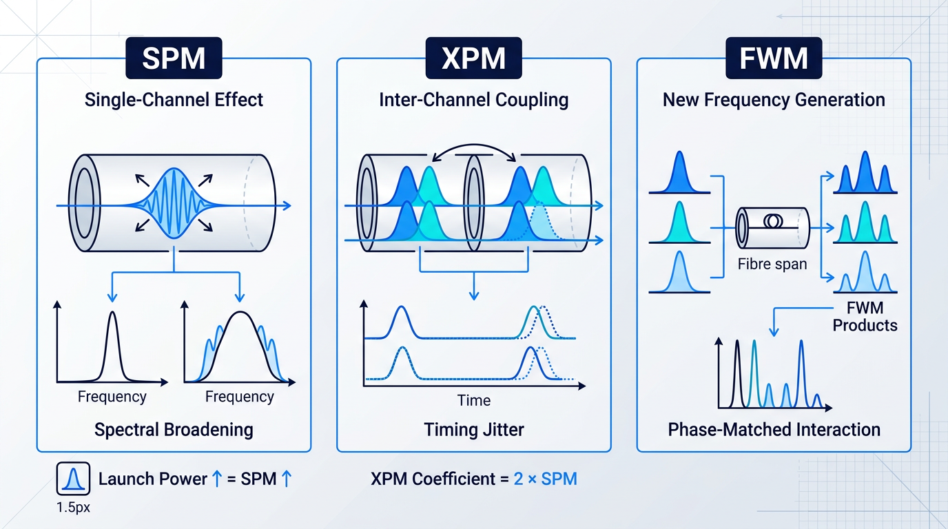
Self-phase modulation (SPM) arises because a propagating signal pulse modulates its own phase as its instantaneous intensity varies across the pulse envelope.
This intensity-dependent phase shift generates new frequency components, producing spectral broadening of the pulse.
When SPM acts alone, spectral broadening is manageable; combined with chromatic dispersion, however, it causes pulse distortion — spreading or compression depending on the dispersion regime — that accumulates across successive spans.
SPM severity scales directly with launch power and inversely with the fibre effective area: a smaller core concentrates the same power into a higher intensity, amplifying the nonlinear phase shift. Crucially, SPM is a single-channel effect and does not require WDM to be problematic.
Cross-Phase Modulation
In WDM systems, each channel experiences not only its own SPM-induced phase shift but also phase modulation imposed by every co-propagating channel — an effect known as cross-phase modulation (XPM).
The XPM-induced refractive index change for a given channel is described by Δn⁽²⁾ = 2·n₂·I⁽¹⁾, where I⁽¹⁾ is the intensity of the interfering channel — the factor of 2 confirming that the XPM coefficient is twice the SPM coefficient for co-polarised channels in single-mode fibre.
This means XPM is, per unit of interfering power, a stronger perturbation than SPM for the affected channel, producing inter-channel crosstalk and timing jitter as pulses from different channels walk through one another at slightly different group velocities.
The severity of XPM depends on channel spacing, launch power, and dispersion — which governs the walk-off rate between channels. Tightly spaced channels with low dispersion walk off slowly, maximising the interaction length and worsening the crosstalk penalty.
Four-Wave Mixing
Four-wave mixing (FWM) arises from the χ⁽³⁾ (third-order) nonlinearity of silica: when two or more WDM channels co-propagate, they interact to generate new frequency components at combinations of the original channel frequencies.
If these new components fall on existing WDM channels, they cause coherent interference and direct signal degradation.
FWM efficiency depends critically on phase matching: the newly generated components must remain in phase with the pump channels over a significant propagation distance for efficient power transfer to occur. Phase matching is best — and FWM most severe — near the zero-dispersion wavelength, where group velocity dispersion is small and channels at different wavelengths travel at nearly the same speed.
This is the engineering reason why non-zero dispersion-shifted fibre (NZDSF) was developed for WDM systems: a small but non-zero residual dispersion disrupts phase matching and suppresses FWM, without introducing the excessive pulse broadening that would result from high dispersion. FWM is the impairment that most directly shaped fibre design choices for dense WDM.
Scattering Impairments: SBS and SRS
Alongside the Kerr-effect impairments, two scattering processes impose additional power-handling constraints in amplified systems, each with distinct characteristics and engineering implications.
Stimulated Brillouin Scattering
Stimulated Brillouin scattering (SBS) is a backscattering effect driven by the interaction between a narrowband optical signal and acoustic phonons in the fibre via electrostriction: the signal generates a counter-propagating acoustic wave, which in turn scatters light backward.
The Brillouin gain spectrum in standard silica single-mode fibre is extremely narrow, with a bandwidth of typically 50–100 MHz — a tiny fraction of the optical frequency, as confirmed by multiple authoritative sources including RP Photonics and the UCSB ECE228 graduate lecture notes.
Above the SBS threshold, backscattered power rises steeply and the forward-propagating signal is effectively clamped: power is transferred backward rather than delivered to the receiver, limiting the maximum launch power for a single narrowband channel.
Because the Brillouin gain bandwidth is so narrow, SBS is primarily a concern for narrowband or continuous-wave signals with linewidths well below 100 MHz. Broadband modulated signals spread their power spectral density across a linewidth that exceeds the Brillouin gain bandwidth, substantially raising the effective threshold.
Suppression techniques exploit this linewidth dependence: phase modulation or frequency dithering of the source laser broadens the signal spectrum beyond the Brillouin gain bandwidth, reducing peak Brillouin gain and raising the threshold. Direct modulation achieves a similar effect through spectral broadening.
Stimulated Raman Scattering as a System Impairment
Stimulated Raman scattering (SRS), the same scattering process that underlies Raman amplification, also acts as an unwanted power-transfer mechanism in WDM systems — and the two roles must be clearly distinguished.
In a WDM system spanning a wide wavelength range, shorter-wavelength (higher-frequency) channels act as unintentional Raman pumps for longer-wavelength (lower-frequency) channels, continuously transferring power from short to long wavelengths along the fibre span.
The result is a power tilt across the WDM band: short-wavelength channels lose power and suffer OSNR degradation, while long-wavelength channels gain power and experience worsened nonlinear impairments.
This SRS tilt becomes significant as channel count and wavelength span increase, and it is an impairment that amplifier gain-flattening cannot fully correct — because it occurs continuously and distributedly along the fibre span, not at the discrete amplifier sites where gain equalisation is applied.
The data table below summarises the key characteristic parameters of the two scattering impairments for comparison.
| Parameter | SBS | SRS |
|---|---|---|
| Scattering direction | Backward (counter-propagating) | Forward (co-propagating) |
| Gain bandwidth (silica SMF) | Typically 50–100 MHz | ~THz-scale (broad) |
| Frequency shift (silica, 1550 nm) | ~10–20 GHz | ~13 THz (~100 nm at 1550 nm) |
| Primary concern in WDM | Per-channel launch power limit (narrowband signals) | Inter-channel power tilt across wide wavelength span |
| Suppression approach | Linewidth broadening via phase modulation or dithering | Gain equalisation; careful power and span management |
Comparison of SBS and SRS scattering impairments by key characteristic parameters relevant to amplified WDM system design.
The contrast between SBS and SRS reflects fundamentally different engineering challenges: SBS sets a hard per-channel power ceiling that is most severe for narrowband sources, while SRS imposes a system-wide power redistribution that worsens as channel count and wavelength span grow.
Mitigation Strategies
System designers address these nonlinear impairments through a combination of fibre design, link architecture, and analytical modelling — each targeting the physical mechanisms described above.
- NZDSF and dispersion management: Non-zero dispersion-shifted fibre provides small but non-zero local dispersion, disrupting FWM phase matching while keeping pulse broadening manageable across multi-span links.
- Large effective area fibre: Fibre designs with a larger core effective area reduce optical intensity for a given launched power, directly attenuating all Kerr-effect nonlinearities including SPM, XPM, and FWM.
- Optimal launch power: Operating at the power level that balances OSNR improvement against nonlinear noise penalty — the system optimum where total noise is minimised.
- Gaussian noise (GN) model: A modern closed-form analytical framework treating accumulated nonlinear noise as approximately Gaussian, enabling quantitative system planning without empirical trial-and-error.
The Gaussian noise (GN) model deserves particular attention as the engineering tool that has transformed coherent WDM system design. By treating accumulated nonlinear noise in dispersion-uncompensated coherent links as approximately Gaussian-distributed, it enables closed-form estimates of nonlinear SNR degradation as a function of launch power, span length, and channel count.
Rather than relying on empirical measurement campaigns to characterise each link configuration, system designers can use the GN model to predict the nonlinear noise floor analytically and identify the optimal launch power for a given link before deployment.
Every optical amplifier in a chain improves OSNR by restoring signal power — but simultaneously sustains the intensity conditions that drive SPM, XPM, FWM, and scattering impairments across the full link. There is no configuration that eliminates this tension; system design is the art of finding the optimal operating point between these two competing penalties.
These mitigation strategies are not abstract engineering principles — they manifest as concrete deployment choices in real-world amplified systems, from the fibre type selected for a long-haul WDM route to the per-channel power budget in a submarine cable. Those deployment contexts, and how amplifier technology maps to each, are the focus of the next section.
Applications: Where Optical Fibre Amplifiers Are Deployed
The physics of gain, noise, and nonlinearity only become meaningful when they translate into deployment decisions. Every real optical network is defined by a dominant constraint — whether that is OSNR budget, reliability over decades without maintenance access, integration density, or the sensitivity of a weak return signal — and the amplifier technology chosen for each context is the one whose engineering profile best matches that constraint. What follows maps each major deployment domain to the amplifier technology it demands, and explains precisely why.
Long-Haul Terrestrial Links
EDFA chains are the dominant amplification architecture for long-haul terrestrial fibre, with in-line amplifiers placed at span intervals typically between 80 and 100 km to compensate for accumulated fibre loss across thousands of kilometres.
The defining advantage here is simultaneous WDM amplification: a single EDFA restores the power of every channel across the C-band in one pass, making it far more economical than any per-channel approach at the scale of a 96-channel dense WDM system.
For ultra-long spans where OSNR budgets are particularly tight, system designers turn to hybrid Raman/EDFA configurations: distributed Raman gain in the transmission fibre itself reduces the effective noise figure of the combined amplifier stage by lifting the signal before the lumped EDFA sees it, improving OSNR at the span output without increasing launch power.
The primary system design constraints in long-haul terrestrial links are OSNR accumulation across the amplifier cascade and the nonlinear impairments — SPM, XPM, and FWM — that worsen as launch power increases, creating the fundamental power optimisation trade-off covered in the preceding section.
Submarine Cable Systems
Submarine links impose a reliability constraint that has no equivalent in terrestrial engineering: once a cable is laid on the ocean floor, the EDFAs within it must operate continuously for design lifetimes of 25 years or more, with repair interventions that are enormously costly and logistically complex.
The engineering response to this constraint is visible in every aspect of submarine EDFA design: pump laser redundancy schemes (typically multiple pump diodes in parallel with automatic switchover), hermetic packaging to exclude moisture and mechanical stress, and conservative operating margins that sacrifice peak performance in favour of long-term stability.
EDFA-enabled submarine systems have been in commercial service since the early 1990s, and today's transoceanic cables carry aggregate capacities measured in terabits per second — a scale that would be impossible without the EDFA's ability to amplify all WDM channels simultaneously over spans of thousands of kilometres.
Metropolitan Area Networks
Metro networks differ from long-haul in character as much as in scale: spans are shorter, but the network is architecturally more dynamic, with frequent channel add/drop operations at ROADMs (reconfigurable optical add/drop multiplexers) that cause rapid, unpredictable changes in the number of active channels.
EDFA remains the workhorse amplifier in metro, but dynamic gain control is a critical operational requirement here in a way it is not in long-haul: when channels are added or dropped, the surviving channels experience transient power excursions driven by gain saturation behaviour, which must be suppressed quickly to avoid bit-error-rate penalties.
SOAs find a specific and well-suited role in metro ROADMs as optical gates and switches, exploiting precisely the fast gain dynamics that make them unsuitable for linear WDM amplification — the same sub-nanosecond carrier lifetime that causes cross-gain modulation in a WDM amplifier becomes an asset when the device is used to switch or gate individual channels on microsecond timescales.
Datacentre Interconnects
The datacentre interconnect (DCI) context is the primary deployment domain where SOAs integrated into photonic integrated circuits (PICs) are preferred over EDFA for short-to-medium reach amplification.
The engineering rationale is form factor and integration: SOAs are electrically pumped, requiring no separate pump laser, and their semiconductor structure is directly compatible with silicon photonics platforms, enabling co-integration with modulators, detectors, and routing elements on a single chip at the density that datacentre economics demand.
For longer DCI spans where the SOA's higher noise figure becomes a limiting factor, EDFA remains the preferred choice — its superior noise performance justifies the added complexity of a separate pump laser when the link budget requires it.
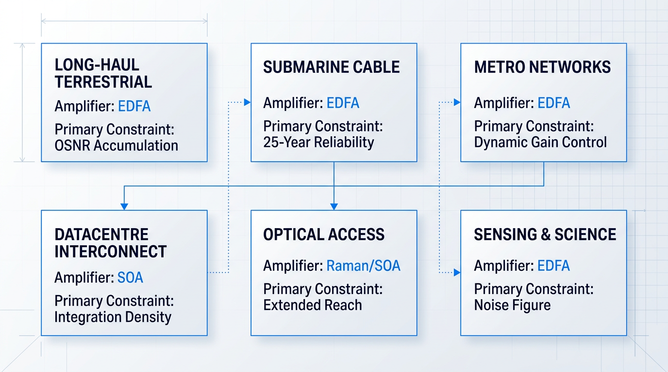
In every deployment context, the amplifier technology selected is the one whose engineering profile matches the dominant system constraint: OSNR budget in long-haul, reliability in submarine, switching speed in metro ROADMs, integration density in DCI, and noise figure in sensing. No single technology is universally superior.
Optical Access Networks
In passive optical networks (PONs), distributed Raman amplification offers a means of extending reach beyond standard loss budgets by generating gain within the access fibre itself — a niche application that demonstrates Raman's wavelength flexibility and distributed gain advantage where a lumped amplifier would be impractical to site.
SOAs serve a complementary role at the optical line terminal (OLT) as booster amplifiers, increasing the available power budget to support higher split ratios and larger subscriber counts without requiring additional fibre infrastructure.
Sensing and Scientific Applications
In sensing applications — including LIDAR, distributed acoustic sensing (DAS), and optical coherence tomography (OCT) — the EDFA operates predominantly as a pre-amplifier, boosting a weak optical return signal before photodetection.
The dominant specification in this context is noise figure, not output power or gain bandwidth: the amplifier is the first active element in the receiver chain, and any noise it adds degrades the signal-to-noise ratio of the detected signal irreversibly, directly limiting the range or resolution of the sensing system.
With the deployment landscape mapped across all major contexts, the natural next step is to distil these patterns into a practical framework for amplifier selection — which is precisely what the conclusion addresses.
Conclusion
Choosing and deploying optical fibre amplifiers: key considerations
EDFA, Raman, and SOA each occupy their niche not because one is better than the others, but because each represents a different answer to a different engineering question — and the question is always set by the system, not the component.
The right optical fibre amplifier is the one whose trade-offs align with what the link demands: span architecture, OSNR margin, channel plan, and integration constraints all bear on that choice in ways no datasheet resolves alone.
Understanding why those constraints matter — how noise accumulates, where nonlinear effects bite, how gain flatness shapes usable bandwidth — is what separates a system designer from someone who simply specifies components.
Frequently asked questions about optical fibre amplifiers
Common questions about how optical fibre amplifiers work, the differences between amplifier types, and their role in modern fibre-optic communication systems.
An optical fibre amplifier is a device that amplifies optical signals directly within a length of optical fibre, without converting those signals to electrical form. The signal remains entirely in the optical domain throughout — this is the defining property that distinguishes it from an optoelectronic repeater. Three principal families exist: the erbium-doped fibre amplifier (EDFA), which uses stimulated emission in a rare-earth-doped fibre; the Raman fibre amplifier, which exploits stimulated Raman scattering in the transmission fibre itself; and the semiconductor optical amplifier (SOA), which achieves gain through stimulated emission in a semiconductor active region. Optical fibre amplifiers are the enabling technology of long-haul and transoceanic fibre-optic communication systems, where they restore signal power at regular intervals across thousands of kilometres.
An optical amplifier compensates for signal attenuation — the gradual loss of optical power as light propagates through a fibre span. By restoring signal power entirely within the optical domain, it allows the signal to continue propagating over the next span without degradation. Critically, because no electrical conversion takes place, the amplifier is data-rate transparent and can boost all wavelength-division multiplexed (WDM) channels simultaneously in a single pass. Without optical amplification, long-haul and transoceanic fibre links would not be viable at the channel counts and data rates modern networks require. Repeaters would need to be placed far more frequently and would be tied to a specific bit rate — a significant constraint as network capacity scales.
An optical amplifier boosts the signal directly in the optical domain — no electrical conversion occurs. A repeater (more precisely, an optoelectronic regenerator) detects the incoming optical signal, converts it to an electrical signal, amplifies or regenerates it electrically, then converts it back to optical for retransmission. This difference has significant practical consequences. An optical amplifier is data-rate transparent: it does not need to be redesigned when the bit rate changes, because it has no awareness of the signal's modulation format. It also amplifies all WDM channels simultaneously in a single device. A repeater, by contrast, is both rate-specific and channel-specific — a 100-channel WDM system would require 100 parallel repeaters at every regeneration point, one per wavelength. Optical amplifiers have largely displaced repeaters in long-haul systems since the early 1990s. That said, full 3R regeneration (re-amplify, re-shape, re-time) — which only a repeater provides — remains necessary at certain points in a network where accumulated noise and distortion must be completely cleared rather than merely amplified.
The erbium-doped fibre amplifier (EDFA) dominates long-haul systems for a convergence of reasons that no competing technology fully matches. Its gain band spans the C-band (1530–1565 nm), which coincides precisely with the lowest-loss transmission window of standard silica fibre — meaning the amplifier and the medium it serves are optimised for the same wavelength range. It achieves a low noise figure approaching the quantum limit, it is polarisation-insensitive, and it amplifies all WDM channels simultaneously in a single device without inter-channel crosstalk. A further practical advantage is EDFA's slow gain dynamics, with a response time on the order of 10 milliseconds. This timescale is far longer than the bit period of any realistic data signal, so transient power fluctuations between channels do not cross-couple — a property that greatly simplifies WDM system engineering. The technology is also mature, with decades of deployment experience, well-understood reliability, and cost-effective manufacturing at scale.
An optical fibre amplifier is a type of optical amplifier in which signal gain is produced within a length of optical fibre, typically one that has been doped with a rare-earth element such as erbium. A pump laser excites the dopant ions to a higher energy state; incoming signal photons then trigger stimulated emission, releasing additional photons at the signal wavelength and producing gain. The primary application is fibre-optic telecommunications, where these devices restore signal power over long transmission distances. In common usage, the term most often refers to the erbium-doped fibre amplifier (EDFA), though it also encompasses Raman fibre amplifiers, which generate gain through stimulated Raman scattering in the transmission fibre rather than in a specially doped gain medium.
Optical signals are amplified by three principal physical mechanisms. In stimulated emission within a doped fibre, a pump laser excites rare-earth dopant ions (most commonly erbium) to a higher energy state; incoming signal photons trigger stimulated emission, producing coherent gain at the signal wavelength. In stimulated Raman scattering, a high-power pump laser transfers energy to signal photons via inelastic scattering off the vibrational modes of the glass lattice. In stimulated emission within a semiconductor, electrical current injection creates population inversion in a semiconductor active region; signal photons stimulate electron-hole recombination, generating gain. In long-haul fibre-optic telecommunications, the first mechanism — implemented as the erbium-doped fibre amplifier — is by far the dominant approach. Raman amplifiers serve as a complement in high-capacity or ultra-long-haul systems, while semiconductor optical amplifiers are used in specific applications such as optical switching and short-reach photonic integration.